On this moment There are also several types of connectors for installing RAM. Such as: SIMM, DIMM, RIMM.
SIMM(Single In line Memory Module - a memory module with one row of contacts) - a memory module inserted into a clamping connector. In addition to the computer, it is also used in many adapters, printers and other devices. SIMM has contacts on both sides of the module, but they are all interconnected, forming, as it were, one row of contacts. SIMM modules come in two types (30 and 72 pin). The main difference is in the number of contacts on the module. But 30 pin "new modules have been out of production for a long time and most likely you will not find them.
DIMM(Dual In line Memory Module - a memory module with two rows of contacts) - a memory module similar to SIMM, but with separate contacts (168 pin, i.e. 2 rows of 84 pins). Contacts are located on both sides, but are galvanically separated, unlike SIMM modules. This increases the bit depth or the number of memory banks in the module. Also, connectors of a different type are used than for SIMM modules.
CELP(Card Egde Low Profile - a low card with a knife connector on the edge) - an external cache memory module assembled on SRAM (asynchronous) or PB SRAM (synchronous) chips. By appearance similar to a 72-pin SIMM, has a capacity of 256 or 512 KB.
Connectors for connecting external devices
USB(Universal Serial Bus - universal serial bus) - one of the modern interfaces for connecting external devices. Provides connection to 127 external devices to one USB channel. The principles of building USB are similar to the principles of building a common bus. Hardware implementations typically have two channels per controller. Interface exchange - batch, exchange rate up to 12 Mbps.
LPT(LinePrinter) - was originally designed to connect a printer to it, but later a number of devices appeared that could work through the LPT port (scanners, Zip drives, etc.). An LPT port is an 8-bit parallel port plus 4 status bits.
Operating modes of the parallel LPT port
SPP(Standard Parallel Port) Provides 8-bit data output with polling or interrupt clocking. The maximum output speed is about 80 KB/s. Can be used to enter information on status lines. The maximum input speed is about half that.
EPP(Enhanced Parallel Port - extended parallel port) - high-speed bidirectional interface option. The purpose of some signals has been changed. Introduced the ability to address multiple logical devices and 8-bit data input. A 16-byte hardware FIFO buffer is used. The maximum exchange rate is up to 2 MB/s.
ECP(Enhanced Capability Port) is an intelligent version of EPP. The possibility of dividing transmitted information into commands and data is implemented, as well as support for DMA and compression of transmitted data using the RLE (Run-Length Encoding) method.
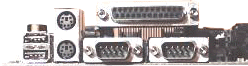
COM port - serial port. Exchange rate up to 115 Kbps. Only one device can be connected to a port. It is mainly used to connect a mouse or modem. Standard in motherboard built-in two serial ports.
PS/2 port - serial port. It is a functional analogue of a COM port, but has additional lines for powering connected devices. Used to connect a keyboard or mouse.
Memory
There are several types of memory in a computer: cache memory, RAM, video memory, external memory. There are also devices with built-in memory, which users often do not know about. This memory resides on the clipboard and is intended to speed up the I/O operation (for example, for disks) or to keep it until the processor requests it (for example, from the keyboard). Registers in the CPU are also areas of memory.
external memory called memory, which is located outside the motherboard and includes disk memory (on floppy and hard disks), magnetic tape memory, memory on a sound card, printer memory, etc., that is, almost every device has its own memory. These types of memory will be discussed in the relevant sections. Memory in the form of registers, how it is arranged and how it works - this is specific information and does little to understand the work on a computer if you are not system programmer and therefore not considered here. Now let's take a look random access memory.
RAM
One of the main components of a computer is working memory b, which serves as a place to store information and for its further transfer to the processor, hard drive, and other external devices. It is located in special slots on the motherboard. RAM is the place where data and instructions are stored with which the central processor works, and is a circuit of a huge number of tiny capacitors and transistors (one such pair can usually store one bit). Therefore, when you turn off the computer or suddenly turn off the power, it turns out that the information you just entered is gone. This is because the data has not been written to HDD, where they can be stored for a long time, but were in RAM. If there were no RAM, then the data would be located on the hard disk and the access time would increase dramatically, which would lead to a sharp decrease in the overall performance of the computer.
RAM is also referred to as RAM (Random Access Memory - random access memory). The concept of random access means that you can access an arbitrary memory cell, in contrast to the sequential access method, when in order to access a cell, you must first read other data that is before this cell (an example is a magnetic tape).
RAM is made in the form of chips mounted on special plates that are installed on the motherboard in the appropriate slots. When you turn on your computer, the operating system is loaded into RAM, then application programs, such as Word, and data, such as documents, are loaded into it. The central processor manages the loading of the program, data into RAM, then work with the data in RAM, and not on the hard disk. If data is required that is on the hard disk, then the information is first loaded into RAM, after which it is called for processing by the central processor. After processing, it is again placed in RAM and then stored on the hard disk. That is, the central processor works with instructions and data that are in RAM, and all other devices (disks, magnetic tape, modem communication, etc.) operate through it. Therefore, RAM has a huge impact on the performance of a computer. Since RAM is designed to store data and programs only while the computer is running, after turning off the power, all the data that was in it is lost. Therefore, before turning off the computer, you need to save data to the hard drive, for which you should exit applications.
Data transfer between the RAM and the processor occurs on the system bus, which is characterized by a clock frequency, that is, the number of cycles per second. This indicator is measured in megahertz, that is, the number of millions of cycles per second. The amount of data that is transferred during one bus cycle is called the bus width. Compared to the processor, the performance of RAM is less, and so that the central processor does not stand idle, a cache memory is organized that is faster than RAM and stores an image of RAM sections. If hard disks were much faster, RAM might not be required, but hard drives are about 200 times slower.
There are several types of RAM, but the main types are SDRAM (Synchronous Dynamic Random Access Memory - synchronous dynamic random access memory):
DDR(Double Data Rate - double data rate). Double the speed is achieved by reading data not only on the edge (signal rise), but also on the fall of the signal. Thus, two data bits are transmitted in one cycle, that is, if the system bus frequency is 100 MHz / s, then we get an effective frequency of 200 MHz / s. The data bus width is 64 bits, that is, for the previous example, we get a bandwidth of 100 MHz x 2 x 64 bits = 12.8 Gbps. Microcircuits are made according to the technology of 0.13 and 0.09 microns of the process.
There are the following types of memory: DDR 200 to operate at 100 MHz, DDR 266 at 133 MHz, DDR 333 - 166 MHz, DDR 400 - 200 MHz, DDR 433 - 217 MHz, DDR 466 - 233 MHz, DDR 500 - 250 MHz , DDR 533 - 267 MHz. Boards may have another name that starts with PC with a rounded memory bandwidth value. So DDR 200 memory can be called PC1600, DDR 266 memory is called PC2100 (bandwidth - 2133 megabytes per second), DDR 300 - PC2400, DDR 333 - PC2700 (bandwidth - 2667 MB / s), DDR 400 - PC3200, DDR 433 - PC3500 (3467Mb/s), DDR 466 - PC3700, DDR 500 - PC4000, DDR 533 - PC4300 (4267Mb/s). Bandwidth indicated in single-channel mode, in dual-channel this figure is doubled. Most boards allow you to work in two-channel mode, but there are also four-channel modules.
The above frequency indicates the guaranteed frequency at which the module operates. The module can be used at lower (this is called underclocking or underclocking) and higher frequency (overclocking or overclocking).
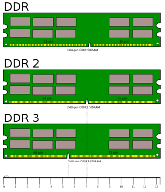
The figure above schematically shows a DDR memory board. On the board, on both sides, there are microcircuits with memory; in the figure, there are eight of them on one side. On the left and right are two recesses for installing the board into the slot on the motherboard. Below is the key (notch on the board). Since there is a partition in the slot in place of the key, it must enter the key. If the key is in a different place, then the partition will prevent the board from being inserted into the slot. There are also contacts on the bottom, to the left of the key - 52, to the right - 40 contacts, a total of 92 on one side. Since the contacts are located on two sides of the board, their total number is 184.
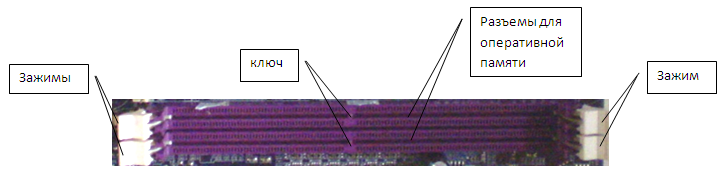
The figure above shows two slots for installing RAM. As you can see, not far from the middle of the connector there is a bulkhead (in the figure it is named as a key).
The main characteristic of a RAM board is its capacity. It is measured in megabits. If one chip has a capacity of 512 Mb, then the total capacity on this board will be 512 x 8 (8 chips on one side) x 2 (2 sides of the board) = 8194 megabits = 1024 megabytes = 1 gigabyte. Thus, the board in the figure has a capacity of 1 gigabyte.
As you can see in the figure, there are 8 microcircuits on the board on one side, that is, there will be 8 microcircuits per 1 byte, each of the microcircuits will contain 1 bit. Such boards are usually found on home computers.
However, there are boards on which there are nine microcircuits, that is, 9 bits per byte. The ninth bit is used for ECC(Error Checking and Correcting - detection and correction of errors). The idea is pretty simple. If we sum all eight bits, we get an even or odd number. If the number is even, then the ninth bit will be 1, if odd, then 1. Thus, the sum of all nine bits will always be odd. If an error occurs and one bit is inverted, that is, it will be equal to 0 instead of 1 or 1 instead of 0, then the sum of all bits will be equal to an even number and the system signals an error. For what reasons can a bit be changed? Because of magnetic fields, because of cosmic rays and radiation. These errors are quite rare, but for some systems, for example, those that support the banking system, they are extremely important. These changes are tracked at the hardware level. Unfortunately this method does not allow you to determine which bit was inverted, and in the case when two bits are inverted, the method will not detect this. Therefore, a method was developed Chipkill, which allows you to determine at the hardware level which bit was inverted and correct it. Moreover, to determine the error of not one, but several bits. There are also other methods for correcting errors - memory scrubbing , Intel SDDC .
Chips can be 4 (x4) or 8 (x8) bit wide, with x8 bit being cheaper and not allowing Chipkill, memory scrubbing, and Intel SDDC methods.
DDR 2 the second generation of this type of memory, which appeared in 2004. The difference from DDR is twice the bus frequency over which data is transferred to the buffer. The main difference is that this type of memory can operate at a higher frequency, since DDR had a limitation. Tests show that the speed of DDR 2 is slightly higher than that of DDR, approaching the declared one.
The fees are also different. The key is shifted to the left, there are 64 pins to the left of the key, 56 to the right, in total on one side - 120, in total on two sides - 240. Thus, DDR memory cannot be inserted into the DDR 2 slot and vice versa, that is, they are not interchangeable.
DDR 2-400 (PC 2-3200), DDR 2-533 (PC 2-4200), DDR 2-667 (PC 2-5300), DDR 2-675 (PC 2-5400), DDR 2-700 modules available (PC 2-5600), DDR 2-711 (PC 2-5700), DDR 2-750 (PC 2-6000), DDR 2-800 (PC 2-6400), DDR 2-888 (PC 2-7100) , DDR 2-900 (PC 2-7200), DDR 2-1000 (PC 2-8000), DDR 2-1066 (PC 2-8500), DDR 2-1150 (PC 2-9200), DDR 2-1200 ( PC 2-9600).
DDR 3 the third generation of this type of memory. The difference from DDR 2 lies in the reduced power consumption (by 40%), since there was a transition to 90, 65, 50, 40 nanometer technologies (one ninometer is equal to one thousandth of a micrometer).
The fees are also different. The key is shifted even more to the left, there are 48 pins to the left of the key, 72 to the right, in total on one side - 120, in total on two sides - 240. Thus, DDR 2 memory cannot be inserted into a DDR 3 slot and vice versa, that is, they cannot interchangeable.
DDR 3-800 (PC 3-6400), DDR 3-1066 (PC 3-8500), DDR 3-1333 (PC 3-10600), DDR 3-1600 (PC 3-12800), DDR 3-1800 modules available (PC 3-14400), DDR 3-1866 (PC 3-14900), DDR 3-2000 (PC 3-16000), DDR 3-2133 (PC 3-17000), DDR 3-2200 (PC 3-17600) , DDR 3-2400 (PC 3-19200).
DDR 4 the next generation of this type of memory, which is planned to be mass-produced in 2013. This type memory will support frequencies from 2133 to 4266 MHz / sec.
Memory is organized in blocks of 8 bits, which make up 1 byte. To increase memory reliability, a ninth bit is sometimes added, called parity bit, which takes on a value in such a way that the sum of all nine bits is a certain value modulo two (0 or 1), and violation of this rule means a memory error. If it is present, a message will appear on the screen stating that a parity error has occurred. However, not all chips have 9 bits, since not all memory modules use this method and such chips are slightly cheaper than parity. Some manufacturers use 8 bits to reduce the cost of chips, calculate the value of the ninth and send the value of 9 bits to the processor, and such chips are difficult to distinguish from 9-bit ones.
Some manufacturers produce chips with error correction according to the same principle as it is done in hard drives, that is, in some cases they allow you to restore corrupted information. This memory uses an additional 7 bits (ECC) for 32 bits and 8 for 64 bits. Such memory is more expensive and is used for computers that require special data storage reliability. If errors occur frequently, you can use special programs to determine the location of failures. Usually, home computers use memory without parity and ECC codes, since the operation of the memory is already quite reliable. If errors occur, you can restart the computer to get rid of the induced errors and, in addition, perform memory tests from time to time.
RAM is not all composed of rewritable memory cells (RAM or Random Access Memory). Part of the RAM consists of non-rewritable cells (ROM or ROM - Passive Memory Device), it does not allow you to write information to it. The data and programs recorded in it are installed once and do not change for a long time. This type of memory is used by the BIOS and is required when the computer is turned on so that the operating system can be started after the power is turned on.
There is also memory in the BIOS, which stores the most important parameters of the computer system, which can be adjusted. After turning off the power supply, they are supported by the energy of electric batteries or accumulators that are installed on the motherboard. The energy of these batteries allows you to work and the system clock, which works when the computer is turned off. Memory that uses battery power is different types, but it is quite expensive and as RAM is not used.
When turning on the computer The processor accesses the contents of memory located at 1MB -16, where the first instruction to be executed is located. Naturally, this cell contains ROM memory (read-only), otherwise it would not have been saved. The first megabyte of RAM is well defined: at the very beginning there is a table of interrupt vectors, data for the BIOS or DOS, the operating system. Then follows a memory area that is used for user programs, up to 640 kilobytes in size, the end of the memory (up to the first megabyte) is allocated for the BIOS video buffer and other operating system purposes. One of the differences between RAM and other devices is that after installing it, the computer itself finds and tests it, no installation of drivers and new software is required. The first procedures after turning on the computer are described in more detail below.
After turning on the computer starts working special program BIOS POST, with the first kilobyte of memory reserved for the interrupt vector table (IVT), and the top of the first megabyte contains the operating system boot program (BIOS). This program fills in the interrupt program addresses in the IVT table and the data in the second kilobyte of memory, after which it loads boot program into memory at address 700h, and control is passed to it to load the operating system. Then the interrupt program and the operating system kernel are loaded, the boot program is replaced, then the operating system kernel starts configuration files Autoexec.bat and Config.sys (or Windows files).
The DOS operating system has a special table called a list of lists, which has a pointer to the first MCB table, which specifies the memory allocation for programs. Moreover, the first block of the MCB indicates the allocation of memory for DOS itself, and the rest - for applied tasks. One task can own several such tables, while one table belongs to only one program. This table defines the memory of the first 640 kilobytes, hence the problem for some old programs in the 640 kilobyte boundary. When the application program terminates, the used memory is returned by the application program to the operating system. If the program has finished running, but remains in memory, then such a program is resident. An example of such a program is a mouse program. Each MCB is in front of the described area. The block has 16 bytes of data, which include the block type, identifier (if 0, then the memory described by the block is free) and other data. In order to view the MCB chain, you can use the Debug or Mem program with the /d switch.
After turning on the computer, it works in real time. Then Windows 9x boots up and goes into protected mode. When emulating the DOS mode, the program is allocated the memory it needs and an interrupt vector table is created, the operating system emulation programs, the drivers and programs it needs are loaded, after which the program itself is loaded, which starts executing. It seems that it works in real time, but in fact - in a protected one. If you call in parallel with it another DOS emulation mode, then new task another area of memory will be allocated again, where the program will work with the creation of the environment necessary for it. Work in the Windows system occurs only in protected mode. However, early Windows systems The 9x occasionally go into real mode, accessing DOS to perform low-level system actions, but immediately go into protected mode after doing so.
The only exception to this rule is the transition in the Windows 98 system using the command Start → Shutdown → Restart the computer in emulation mode MS-DOS, at which there is a transition to the real mode of operation.
The more applications running, the more memory is required for them. In addition, there may be applications that themselves use a large amount of memory. If there is not enough RAM, then some of the information is moved to a temporary file on the hard disk, and this happens with areas that are rarely used. This reduces the performance of using these areas, but allows you to perform a large number of tasks at the same time and improves the performance of your computer. Therefore, the more RAM in the computer, the less information needs to be dumped on the hard drive and the faster the computer works.
RAM is divided into five areas, and this division has been preserved from the first personal computers. At that time, a memory of several hundred kilobytes in size seemed very significant in terms of its volume, and the first XTs were produced with a memory of no more than 640 KB. This area of memory is called standard, basic, basic memory or ordinary RAM ( Conventional Memory), in which the beginning of the area is given to the operating system, and the rest is for the operation of programs. In this case, the first kilobyte is intended for the interrupt vector table, then the BIOS data area is located, and then the operating system kernel program. After the expansion of computer memory to 1 megabyte, which could be accessed using the base:offset addressing type, a memory area from 640 kilobytes to 1 megabyte, called UMA(Upper Memory Area or sometimes Extended Conventional Memory ), or upper memory, or older memory was used to run the operating system. It contains buffers for the graphics adapter, BIOS programs, buffers for page memory. In order to make full use of the area of the first 640 KB, many programs and drivers are loaded into the upper part of the memory, which is located from 640 kilobytes to one megabyte. This is done in a DOS system using the DOS =UMB command in Config .sys and the Lh and Dh commands that load drivers into this area. When working with Windows, many of these problems are solved automatically.
Upper memory allotted: A 000-BFFF video memory (not fully used), C 000-C 3FF for EGA video adapter, BIOS ROM , C 000-C 7FF for VGA video buffer, BIOS RAM, C800-CBFF contains BIOS hard disk, F 000-FFFF – BIOS , F 000-F 0FF – area for configuring Plug & Play, C000h -BAAAh – for adapters with their own ROMs BIOS.
Memory over 1 megabyte is called extended or additional (XMS or Extended ) memory. The first 64 kilobytes over the first megabyte is called HMA . This area can be accessed in real mode. On early computers, when accessed at FFFF :000F there was a transition to the zero address (0000:0000), that is, the memory was represented cyclically. Over time, the address above the first megabyte began to access data that is more than one megabyte, and not to the zero address, and thus these 64 kilobytes began to be used in real mode.
In order to use memory over 1 megabyte, special system utilities Himem.sys and Emm386.exe in the Config.sys file, where 64 kB memory over 1 megabyte is supported by the Himem driver. These drivers are required for DOS and Windows 3.11 systems. With their help, the extended memory area is displayed on 4 pages of 4 kilobytes in a special buffer in the upper area of the first megabyte (page mode). Currently, memory accesses over one megabyte are used in protected mode, which is supported on Windows 95 and above.
It occupies a special place video memory. In early models, when mostly text information was displayed, the video buffer was in the upper area of the first megabyte of main memory and occupied 16, 32 or more kilobytes of memory. However, with the advent of high-resolution graphics modes, the video buffer required a significant amount of memory, which began to be located on the video card. It already occupies 64, 128, 256 or more megabytes of memory.
A buffer with a maximum size of 128 kilobytes has been preserved in RAM, which displays part of the video memory in the video card located in the video buffer. The central processor works with this buffer, and it can display fragments of video memory there for processing at different times.
The video memory itself is located on the video card (or on the motherboard, if the video subsystem is integrated into the card) and is required in order to create a screen image and transfer it to the display. Since the image is updated several dozen times per second, while the image is being displayed from one screen frame, the next one starts to be processed in another part of the memory. With a lot of processing of graphic information, some of the calculations can be given to a special processor, which is located on the video card, for example, for such purposes as calculating elementary image objects, which is often used in video games. How more powerful processor on the video card, the better the image is displayed on the display.
IN real mode work, the application program can use all the capabilities of the computer, with virtually no restrictions. IN protected mode the case is somewhat different. The physical address is not calculated directly, but using special tables. The computer has four priority levels, with the zero level belonging to the operating system itself and having almost the same capabilities as in real mode. Levels 1 and 2 have fewer features and are hardly used today. The last, 3rd level is used for application programs. A program of this level has fewer opportunities to interfere with the operation of the operating system, however, for its work, for example, when accessing a disk or other device, it can receive the required data from the operating system. This assumes that the operating system is more reliable than the application program, which is confirmed by practice.
Restrictions are laid, first of all, in the address translation procedure itself, since special tables are used in this case, which contain fields with access rights and request privilege level bits that determine what can be done by the program in a given memory area. The DOS system works in real mode, the Windows 95 and higher system works in protected mode, that is, the Windows system allocates all the memory available on the computer for application programs, which it allocates itself.
At work in multitasking mode there is frequent switching between tasks, when the operating system allocates a certain period of time to one task, then another, then a third, again the first, etc. These periods of time are extremely short and repeat many times in one second, so that it seems to the user that all programs are running at the same time, namely, music sounds, the printer displays a page, a character is entered from the keyboard into the text of a document, etc.
To transfer control from one task to another, Current state task (more precisely, the main registers in the central processor) is stored in a special area of \u200b\u200bmemory called stack and in RAM. Then the stored values of another task are called into the registers of the central processor and control is transferred to them.
To whom and for how long to transfer control, the operating system decides depending on the algorithm that was invested by the developers when writing it. There can be two different modes of program operation. In the first case, the processes are equal, and in the second, one process has an advantage over the other and is called background. In the latter case, the program receives control when the main program is waiting, for example, for input from the keyboard, that is, it uses those time intervals when the main program is free.
During a call to a subroutine or switching from one task to another, it is required to temporarily place the current values, for example, those that were in registers, in some memory area. That is, it is necessary to remember the state of the task at the current time, so that later, restoring them, continue the program execution. For this organized stack system. Its idea is simple. In the memory area, an area is allocated for organizing the stack. A special register points to the current position on the stack, and when data is pushed or popped there, it is incremented or decremented by the length of the data. The stack uses the “last in, first out” principle, that is, the last incoming data is selected, then the penultimate one, and so on. Actions for the purpose of data sampling are carried out by the programmer when writing the program. If the stack is full, that is, there is not enough space for data, an error occurs and a message about it appears on the screen, and the task is terminated. As a rule, this does not mean that the computer is not working or broken, it is best to restart the computer and start working again. If given error will continue in the same program, and other programs work fine, then the program is to blame, not the computer. Of course, such an error can also occur due to the fault of the computer, for example, due to bad RAM, but this is quite rare.
How much RAM is required in computer? The bigger, the better. It all depends on the applications with which the user works. If there are a lot of them and work is done with graphics or video, then a significant amount of memory is required. It is desirable to have at least 32 MB for Windows 98, and 64 MB or more for several applications. Windows XP requires significantly more RAM. For her, it is desirable to have 512 megabytes, and preferably 1 gigabyte. Next OS(Windows Vista, Windows 7) require even more memory. Therefore, for these systems, you need to have at least 1 gigabyte, and preferably 2 or 3 gigabytes. We are talking about 32-bit systems, which are mostly common. For 64-bit systems, the memory size must be multiplied by 2, that is, for Windows 7, you need to have at least 2 gigabytes, better 3-4. The more memory installed, the better the performance of the computer will be, especially since memory prices are steadily falling.
If a message appears on the screen Parity error, then among the reasons most often a memory failure. In this case, log out of Windows and log in again. If this message appears frequently, check BIOS settings. You can also reinstall the memory, that is, remove it and reinsert it. If the errors continue again, then use the test program to check the memory.
Main Features RAM are: access time (time of the read / write operation, that is, the time from the beginning of the read cycle to the receipt of data at the output), its size, performance, bit depth, etc. Performance is measured in megabytes per second, this is the amount of data that the memory can read and write per unit of time. The width of the memory bus is determined by the number of bits with which a read / write operation can be performed at one time. We will consider these and other parameters in more detail.
Memory organized in the form of a matrix, approximately like a display screen, on which there are columns and lines, where at the intersection each element is a circuit of one or two capacitors and transistors. When read, the address is converted to a column number (CAS) and a row number (RAS). In this case, the contents of the entire line are selected, amplified and transferred to a temporary buffer, from where an element is selected at the address of the column, which is read and transmitted to the output of the microcircuit. Since the capacitors are discharged when moving to the temporary buffer, then their values are restored. When writing, the number of the row and column is given, and the desired value is written to the cell at the intersection of the row and column.
To speed up operations, the microcircuit can have several tables, usually 4, 8 or 16. If the microcircuit can store 1 MB of memory and has 8 I / O lines, then each line serves a matrix of 128 KB or 1 MB, which is called address depth space. In this example, when accessing this chip, it will be able to give out the values of a byte, each bit of which is located in different matrices. The more I/O lines, the more data can be received at the same time.
One of the main parameters is access time to data, which is smaller is better and can be from 40 to 80 nanoseconds. This parameter is often associated with a minimum clock period, which, being equal to 10 ns, corresponds to an access time of 50 ns, 12 ns - 60 ns, etc. If the memory is running slower than the system bus requires, then the computer will run slower because there will be processor wait latencies. Therefore, it is necessary to choose the optimal memory for price and performance.
RAM is mounted in so-called banks ( bank- a set of microcircuits providing the required bit depth). If a 32-bit system bus (486) works, and the microcircuit has 8 I / O lines, then 4 microcircuits are needed (4x8 = 32 lines), and if they are installed on one plate, they make up a bank, the Pentium has 64 lines and therefore 8 chips are required without parity, 9 with parity. A bank is the minimum amount of memory that a processor can access in a single access. The bank can be filled and unfilled, its partial filling is not allowed. If the memory modules are located on a plate that is mounted on the motherboard, then the set of connectors that will contain plates with RAM chips that provide the required bit depth is also called a bank. A bank may contain either one or several connectors on the motherboard. Inside the bank, microcircuits should be selected of the same type and the same volume, preferably from the same manufacturer. Different banks may differ in their characteristics and it is desirable to minimize the differences, otherwise they will not be able to work in concert. Modern computers have RAM in which one bank is located on one plate.
One of the most important characteristics of memory is packet exchange cycle, which appeared in 486 processors and Pentium models. In a normal exchange cycle, an address and one data are indicated; in a burst cycle, an address and several neighboring (consecutive) data are indicated. In this case, the first datum is read longer, and the next ones are faster. The entry 5-2-2-2 means that it takes 5 units of time (system clocks) to read the first datum, and two each for the next. Or, it takes 4 wait cycles to read the first data (one cycle per read operation), and one wait cycle for subsequent cycles (4-1-1-1). When it is written that the access time is 40 ns, then you need to keep in mind that the first memory access corresponds to it, subsequent ones will be faster. The other parameters define the duty cycle time, and if the access time is 50 ns, then the duty cycle will be 20 ns in the 5-2-2-2 notation.
The 33 MHz 486 motherboard uses memory elements with an access time of 70 ns (nanoseconds). Faster boards should work with access memory of 60 ns or less. Pentium boards use memory with an access time of 40 ns or less. Access time is measured in nanoseconds, where 1ns=0.000000001 sec. If the sample size from the chip is 1 byte, then such a chip is called a byte wide, if 4 bits, then a nimble wide (nimble is half a byte or 4 bits).
Memory chips are not installed directly on the motherboard, they are grouped into several modules and mounted on a special plate, called the SIMM (obsolete) or DIMM form factor, which are inserted into a special slot. Often, chip capacity is measured in bits, and wafers are measured in bytes.
On platters, it is desirable to install memory with the same access time, preferably of the same type and one company. Not all slots for RAM need to be inserted plates, that is, you can leave the slots free. For example, 512 MB can be inserted in two versions: either 4 slots of 128 MB each, or in one 512 MB slot. Each platter can have a different amount of memory. There can be several elements on the plate, each of which can contain 256 Kb, 1 Mb, 4 Mb, and some others.
RAM on the motherboard differs from video memory, printer memory and cache memory in that they cannot be interchanged with each other, as they are available in different versions and have their own characteristics, but the principles of their operation are the same.
Types of RAM
RAM is called RAM(Random-Access Memory - memory with random access). In the 70s and 80s, in our country, a series of EU machines (Unified Series) was used, in which the RAM was called RAM (Random Access Memory). Therefore, such a name can still be found in computer literature.
Another kind of memory ROM(Read Only Memory - read-only memory). As the name suggests, it can only be read-only and not writable. A similar memory is used for BIOS memory, where important information is stored that should not be erased. Given memory will be discussed further in other sections.
Memory sharing. RAM is divided into dynamic and static memory:
- SRAM(Static RAM - static RAM) - has fast access to information and does not require regeneration, but somewhat more expensive than DRAM. Mainly used for cache memory and registers.
- DRAM(Dynamic RAM - dynamic RAM) - requires regeneration, and therefore the access time is longer than that of the previous type. Almost all modern RAM modules for personal computers have this standard.
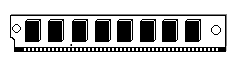
The picture above shows the element DRAM memory. In fact, this is a microcircuit, several of these microcircuits are installed on a plate.
- SD RAM(Synchronous Dynamic RAM - synchronous dynamic RAM) - a subclass of DRAM memory, which has the feature that it uses synchronous data exchange. That is, it allows you to receive commands regardless of whether the previous command was executed or not.
Due to the fact that dynamic memory is cheaper, it is she who is used for RAM. It is made of tiny capacitors and transistors to control the charging process. Physically, the memory is made of a semiconductor material with the formation of elementary cells, in which the information of lines from 1 to 4 bits is stored. The rows are organized into matrices called a page, which in turn create an array called a bank. When information is read, the capacitors are discharged and it is determined whether there was a charge in it or not. If the charge was present, then the capacitor is recharged. Over time, the charge drains, and the stable storage time is measured in milliseconds. In static memory, two transistors are involved per bit of memory, one is on, the other is off, they correspond to two states of memory. At the same time, dynamic memory uses one transistor per bit, so more memory is placed in the same area, but it will work somewhat slower. Therefore, static memory is used for cache memory.
To save information, a rewrite operation is used, which is called memory regeneration at which the capacitors are charged. However, the CPU has access to the data in a refresh-free loop. To coordinate between the RAM and the clock frequency of the processor, there is a parameter - the waiting cycle (Waitstate), which indicates the number of cycles that the processor should skip between two system bus accesses. The greater the number of cycles in this parameter, the slower the computer runs. This parameter is set using the Setup program.
DRAM was used mainly in the 80286 computer and partly in the 386SX. Currently, they are used as composite memory modules SIMM, DIMM, which will be discussed next.
Memory modules can differ from each other by architecture type (Std or FPM, EDO, BEDO and SDRAM), by location type (DIP, SIMM, DIMM and others), by error control method. They may have other differences, for example, different voltage ratings, regeneration parameters, etc.
Error control methods. Memory modules are divided into the following types:
No parity, that is, no error checking. This type is the most common, since the memory works quite reliably;
With parity, that is, checking for oddness, and if errors occur, a signal is sent to the central processor about their presence;
ECC - control with a code that allows you to restore data in case of an error;
EOS - control with a code for recovering information when an error occurs and checking for oddness;
Modules that artificially give out an odd bit by recalculating it, that is, with virtually no parity. They allow you to work on those boards that require parity.
Parity check means the following. Each byte is known to contain eight bits. Some types of memory contain instead of eight - nine bytes, the ninth for parity, that is, the sum of the first eight bytes modulo 2 is taken and this value is placed in the ninth bit. When reading data, if the sum does not match the value in the ninth bit, then an error is generated, which is called a parity error. Similarly, an odd parity check is performed when the value opposite to the sum of the first eight bits is entered in the ninth bit. For example, if there is a value in the first eight bits of “00100100”, then the sum is 10B in binary. The value modulo two is zero. When checking for odd parity, the value “1” (the opposite of zero) will be placed in the ninth bit. For odd parity, the value will be “001001001”. The odd parity check is more often used, since the zeroing of the memory area is detected by this particular check (in this case, the sum of zeros will be even and equal to zero for all nine bits). You can use parity-checked memory on systems that don't require it, but not vice versa.
Thus, if there are 9 microcircuits, then one board with microcircuits serves for parity check, 8 - without parity, that is, the number of microcircuits will be a multiple of 9 or 8 bits of memory. IN Lately, taking into account the reliability of manufactured microcircuits, the parity bit is not used (for example, for 16 MB circuits, one failure for 2-3 years of continuous operation). Memory with parity (Parity - parity) is used in systems where reliability is very critical, that is, in servers that are also constantly loaded. In some cases, when the motherboard requires the presence of a parity bit, it is possible to use RAM chips that emulate a parity bit, that is, they do not actually have a ninth bit and do not perform parity.
There is a memory called ESS that is rarely used, but allows you to correct errors when they occur, that is, when errors occur, it analyzes and can restore a corrupted bit.
Reliability increases with a greater degree of integration. It is taller due to the fact that it has fewer connections, so it is better to buy one 512 MB chip than four 128 MB ones. In this case, you can use not all slots for RAM, but only some, which allows you to further increase the memory.
Memory interleaving is organized in such a way that when a regeneration is performed in one bank (while it cannot be worked with), another bank allows you to perform read / write operations. In this case, adjacent data blocks are in different banks. Due to the frequent reads of sequential data, different banks are used for multiple read/write operations.
Pagination of memory. Addressing is organized like a table, where each element of the table corresponds to an element of memory in the computer, that is, for addressing, you must first specify the row number, then the column. In the case when the next data is adjacent, the row addresses can match, so when an operation is performed on a neighboring cell, only the column address is indicated, which improves memory performance.
Shared memory. Memory that can be accessed by different devices. For example, the adapter's shared memory allows access to it from both the system bus and the adapter.
Shadow memory. Due to the fact that the data that is in the BIOS is read rather slowly, and may be required often, they are copied to the RAM area and then, when the operating system is running, they are read from there, and not from the BIOS. Shadow memory can be implemented by both software and hardware methods.
Non-standard memory. The computer may contain non-standard memory, which is often the case in portable computers. As a rule, many types are common among them, however, it is required to purchase memory only from the manufacturer whose modules are used in the computer. Buying other manufacturers is often cheaper, but they may not be suitable due to special requirements. Memory for portable computers is somewhat more expensive than for stationary ones. Modern laptop models are switching to the use of the types of memory that are used in desktop computers.
IN different types laptops there are holes in different parts of the case for installing RAM, so you need to have the appropriate instructions for them. In more modern laptops, memory is becoming standardized.
architecture type
Architecture was the first FPM DRAM(Fast Page Mode DRAM - fast with a page method), which has two types of memory with different access times: 60 and 70 ns; microcircuits with 60 nsec access operate at a system bus frequency of 60.66 MHz. FPM is also called standard memory and operates in a 5-3-3-3 burst read cycle.
The next modification of memory is EDO DRAM(Extended Data Output DRAM - extended data output DRAM). Speed is achieved through additional registers that store data during the next request to the chip and which allow you to start the next cycle before the previous one ends. Runs 10-15% faster than FPM DRAM. It has access times of 50 ns, 60 ns (for a 66 MHz bus) and 70 ns. Used on motherboards with bus frequencies up to 66 MHz and Pentium processors, less often with a 486 processor. Due to the fact that it is unstable at a system bus frequency of more than 66 MHz, it gradually left the market.
EDO provides pipelining for memory operation. It is used in SIMM-72 and DIMM boards and does not use odd parity, but can remember ECC checksums. This type of memory can be used in both RAM and video memory. To work with this type, the BIOS must be able to work with them, so older motherboards may not support them. Some boards determine the type of memory module using the corresponding BIOS and allow the installation of standard and EDO memory at the same time. Achieves 5-2-2-2 cycle reading in burst mode.
BEDO(Burst EDO - packet EDO) - allows you to read data in blocks or packets in one cycle. Developed from SDRAM and operates at a system bus frequency of 66 MHz. BEDO received further development principles of conveyor processing. This memory takes slightly longer to fetch the first data in burst mode, but provides faster fetching of the next data. It is also used in SIMM-72 and DIMM boards. Achieves 5-1-1-1 in batch read mode.
SDRAM(Synchronous DRAM - synchronous DRAM) - provides data pipeline processing and address interleaving, which increases its performance. All operations in such microcircuits are synchronized with the CPU clock frequency and work with system bus clock frequencies up to 133 MHz, and the operating cycle time is 8-10 ns at a system bus frequency of 100 MHz. For modern buses, there is a PC100, PC133 memory, where the numbers indicate the frequency of the system bus. It works faster than EDO DRAM, but at bus speeds up to 66 MHz, the performance difference is not significant.
SDRAM memory is the most promising, especially for high clock frequencies of the computer's system bus, which other types of memory cannot efficiently support. This memory is installed on DIMM cards or as a chip on a system or video card. Achieves 5-1-1-1 in batch read mode.
SDRAM II(DDR SDRAM) allows access commands to be processed in parallel in their independent memory banks, which speeds up access times. This memory speeds up work by using the rising edge and the pulse decay twice, has the designation PC1600, PC2100, where the numbers indicate the number of MB / s that can be transferred over the bus, respectively 1,600 MB / s using a 100 MHz system bus, and 2100 - for 133 MHz. However, they must be supported by the chipset, which can be consulted in the motherboard manual. More details about DDR, DDR2, DDR3 memory are described above.
Memory Direct RDRAM is a promising memory, to which the by Intel. It can operate at a bus clock rate of 400 MHz/s, with a bandwidth of up to 1,600 MHz/s, allowing data to be transmitted on the rising and falling edges of the pulse, and provides pipelined data sampling. In addition to the above, there is SLDRAM memory, which, like Direct RDRAM, at a frequency of 400 MHz allows data transfer up to 1,600 bytes/sec.
There are modifications of the above types of memory, for example, CDRAM (Cache RAM), EDRAM (Enhanced RAM) - is DRAM memory, which has static memory, is used as a buffer memory in the module. The access time to data in the above types of memory is from 50 to 70 ns.
In addition, there are other types of memory that are installed on graphic (video) cards (but not for RAM) - VRAM , SGRAM , GDDR 2, GDDR 3, GDDR 4, GDDR 5 . Where GDDR 2 is built on DDR 2, GDDR 3, GDDR 4, GDDR 5 are built on DDR 3.
Modern computers use DDR, DDR 2 and DDR 3.
Types of cases, plates. Memory installation
Placement of modules. In older computers, additional cards could be used to increase the RAM up to 32 megabytes. Such memory was installed not with the help of DIMM and SIMM modules, but with the help of a special card, like a sound video card. However, these cards are no longer in production.
In order not to have difficulties with the installation and use of microcircuits, the memory is placed on one plate, which is inserted into a special socket on the motherboard. In older computers, the DRAM module may be made in a dual-in-line package. When installing and removing these elements, care must be taken to ensure that the legs do not bend. To straighten the legs, use thin pliers.
DIP(Dual In-line Package - a case with double-sided outputs) - also an old type of memory, with a capacity of up to 1 megabit, located on the motherboard for models 8086, 286, 386, as well as on graphics adapters. Now they are practically not used for RAM. Their appearance is shown in the figure below. The following types of memory are produced in the form of plates on which memory chips are located.

Modern microcircuits are produced with packages: DIP, ZIP with a zigzag arrangement of contacts, sometimes produced for video memory, SQJ is used in SIMM boards or for special connectors on a video board, TSOP - for installing DIMM on the board.
Modules SIPP(Single Inline Pin Package) or SIP (obsolete). To reduce motherboard space, the DRAM modules are placed on a plate that has 30 pins. The appearance of this board is shown in the figure. Before SIPP, SIP modules were used, but they are hopelessly outdated.

The picture above shows the SIPP board and the picture below shows the SIMM.
Modules SIMM(Single Inline Memory Modules - memory modules in one row), colloquially called "sims" with an emphasis on the last syllable. The SIMM board differs from the SIPP module in that it has a different type of contacts located on the plate, as can be seen in the figure. These modules are equipped with memory chips with 8, 16, 32 or more MB of memory.
All microcircuits that are on the SIMM, DIMM boards are soldered to the board, and it is almost impossible to replace them, so if one module fails, the entire board must be replaced.
For 30-pin SIMMs, you need to use 4 modules for a 486 processor, since one module is 8 bits wide (8 x 4 = 32), and for Pentiums - 8 to provide 64 bits. 72-pin SIMMs are 32 bit wide, so for 486-processors you need to install one board, for Pentium - two. Pentium DIMMs are installed one at a time on the motherboard.
Previously, plates with 30 leads were used. Memory modules currently have 72 pins. The connector where the memory plates are inserted is shown in the figure below.
![]()
To remove it, you need to bend the two clips along the edges of the board and tilt the board, then remove it. The arrows show where to click. Insertion is done in reverse order. The board is brought at an angle and transferred to a vertical position. The clips on the edges themselves are installed in their place, as shown in the figure below.

If you're going to buy a computer and the motherboard has four memory slots, it's a good idea to choose one that doesn't have all the slots filled so that you can add more modules later. the best way to check the health of the memory is to install it in the computer and run the diagnostic program.
At first, such modules used the SIMM standard, then DIMM modules appeared. The SIMM allows you to read one byte at a time. When installing multiple SIMMs, it was often required that they have the same characteristics, follow the same signals, and have the same sampling rate. Often chips with modules from different companies or different types of one company were not compatible with others.
Modules can be single-sided and double-sided, while single-sided, as a rule, have microcircuits on one side of the board, while double-sided, in which there are two banks, the modules are located on two sides.
The Pentium motherboard uses memory banks that work with SIMMs and DIMMs.
DIMM(Dual In-Line Memory Module - memory packed in two rows on the case) has 168, 184, 200 or 240 pins and less access time than on SIMM boards. In addition, the boards overcome the 128 megabyte RAM limit. Now it can reach a significant value, which is indicated in the documentation for the board. The boards contain 2 rows of 92 or 120 contacts (184 or 240 in total, 168 in older computers). Due more contacts, the number of banks in the module increases. The DIMM already has 32 or 64 lines for reading data (4 or 8 bytes, respectively) and it became possible to install them in different computers. Also, DIMMs have more ground lines. The board may contain non-volatile memory, which contains the parameters of the microcircuits. If the required type of microcircuit is missing, then the board will not be able to work with such memory. Unlike SIMM boards, DIMM boards are inserted vertically. Installation of boards of this type of memory is shown in the section on connecting a computer.
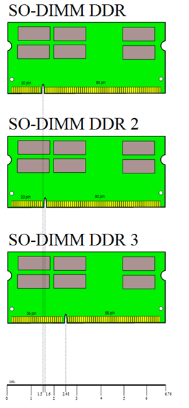
SO-DIMM(Small Outline DIMM - small-sized DIMM) - boards that have 72, 144, 168 or 200 pins and are used for laptops. This memory has 16 independent memory channels and allows you to work with different devices and programs that access different areas of memory at the same time.
There is also a view - DDR 2 Facebook - DIMM, used in servers, RIMM has 168, 184 or 242 contacts and a metal shield to protect the contacts from interference (used for RIMM memory, which is almost out of production), MicroDIMM with 60 pins for subnotebooks and notebooks.
In addition, there is low profile(Low profile ) memory that has a reduced board height for installation in low profile cases. We also note that some boards operating at higher frequencies may have a heatsink in the form of plates.
Memory installation. To install SIMM memory modules, you must first remove the cover of the system unit, remove the old modules (if necessary) and install the boards as described above. Older boards may require jumper settings when adding memory. Next, you need to close the system unit with a lid. When working, be aware of electrostatic electricity, when transporting modules from a store, they must be in antistatic bags; when installing microcircuits, do not touch the contacts with your fingers, as there is grease on the fingers, which can cause poor contact. When installing the modules, do not press hard on them, otherwise the motherboard may be damaged. If installation is inconvenient, it is better to remove the motherboard. If the module does not install, then it may be inserted the wrong way, in which case try turning the module over. SIMM cards are inserted obliquely, while DIMM cards are inserted vertically.
Then you need to check if the system has detected the presence of memory, the size of which can be found in the BIOS program. You can also run a test program to check installed memory whether there are any defects in any microcircuit.
Remarks. Memory chips are significantly smaller than the case in which they are located, however, in order to make it convenient to mount them, and to comply with the temperature regime, this design is used.
A memory expansion card was used for the 286 because the motherboard did not have a dedicated memory slot. This card connected to the system bus and required a special driver with a certain standard, which was called Lim (Lotus, Intel, Microsoft).
The first standard boards for new Pentium processors had, as a rule, two types of memory slots: SIMM and DIMM, each of which is called a bank, and their numbering starts from zero (Bank0, Bank1, and so on), however, many boards do not allow the use both of these types of memory on the board. Banks are filled sequentially, that is, first you need to set Bank0, then Bank1. Thus, it is not possible to set only one Bank1. You can try to determine what memory is on the plate: with parity or not. If there are 8 chips on the plate, then it is without control, if there are nine, then it is with control. It is clear that this is due to the presence of the ninth bit in the byte, which is used for parity. Currently, boards for Pentium processors are only available with DIMM sockets.
There was a special converter board that was inserted into the SIMM slot, and memory modules were inserted into it, that is, if all SIMM slots are occupied, you can install them on the converter and get free slots where you can add additional RAM.
RAM bank numbers are sometimes marked on the motherboard.
In case of malfunction of the RAM, wipe the contacts with an eraser and insert it again, then change the boards among themselves. If the memory worked, then the cause could be a bad connection, since the graphics card consumes a lot of energy and gets quite hot. Therefore, when installing it, you need to place it in such a way that there is free space between it and other boards, preferably near the fan. In this case, you need to make sure that the fan blades do not touch the wires, otherwise it will fail.
Marking. The boards may be marked 1/ /9/ /70, which means 1 - with parity (9 - number of chips), 70 - access time in nanoseconds. The smaller it is, the better, but should be supported by all devices, first of all motherboard.
The last digit often defines the access time in nanoseconds, which can define either the value itself or ten times less. For example, an access time of 70 nanoseconds might be labeled as 70 or simply -7. Values for SDRAM can be -10 (meaning 50 ns), -12 (60 ns), and -15 (70 ns).
In new microcircuits, the name of the manufacturer is indicated first with a few characters, for example, M (OKI), TMM (Motorola), MT - Micron, GM - LG, etc. Each of the companies has a code - a type of cipher, which can be found through the Internet system by referring to the page of the manufacturer.
Cache memory
RAM is not all the memory that is in a computer. In addition to it, there is a cache memory, which is a buffer between the central processor and RAM, which has already been mentioned. The CPU also has a special cache to convert a linear address to a physical address so that it does not have to be recomputed. There is a cache memory for working with various devices (for example, with a hard disk), which allows you to speed up I / O operations, a buffer for the keyboard, etc. All these types of memory are invisible and often not known even to the programmer, since they are implemented at the hardware level .
This chapter will look at cache memory, which works with the processor and is located between the central processor and RAM. The use of cache memory can significantly increase the performance of the computer, as it reduces the idle time of the processor. This is achieved due to the fact that the transfer of data from the cache or to it is faster than to the main memory. If the processor needs to write data to main memory, it writes to cache instead, while the processor continues to run. Further, regardless of the processor's operation, when the system bus is released, data will be transferred to the RAM using the cache controller. In this case, it is possible not only to write, but also to read data from the cache memory.
The effect of the cache memory is effective due to the fact that programs process, as a rule, the same data. In addition, program instructions are located one after another or inside a loop, which increases the likelihood of data being present in the cache. If the required data for reading is in the cache memory, then they talk about getting into it, if the necessary data is not in it, then they need to be read from the RAM and they say about a miss. In general, the essence of cache memory is to save an image of areas from RAM, which is faster.
Principles of organization of cache memory. Direct Mapped Cache (Direct-mapped cache ) partial or set-associative (Set -associative cache ). How does he work? The address of the data to be read is divided into three parts. The first is called tag, the second defines the row, the third column. The cache is organized as a table of lines of a certain length, for example, 1+16=17 bytes each, where the first cell contains the value of the tag, and then there are 16 data values. Having received the address (for example, 123003Ah ), it is divided into three parts: tag (123h), line number (003h) and column number (Ah). In this example, a conditional partition is given, since the dimensions of the numbers may be different. The line number is determined by the number, in our example it is 4 (003h, where - 000h is the first line, 001h is the second, 002h- third, 003 h - fourth, etc.). At the beginning of the line there is a tag value that is compared with the received address tag (123h ). When they match, the data is retrieved or written from the corresponding position (Ah – eleventh value, also 0h – for the first, 1h – for the second, … Ah – for the eleventh); if they do not match, then the required data is not in the cache memory and it is selected from the main memory. This type of cache is used in 386 processors.
Fully associative the architecture can store the data string anywhere in the cache. The address at which the data is read is divided into two parts: the tag and the line number. When a read or write is required, the tags in the entire cache are checked and this one is selected if there is a match. In this method, more steps are required to find the given one, since it is necessary to view the values of all tags in memory, that is, more hardware costs.
Type-associative architecture uses a combination of the above methods and is the most common. In this case, several lines are combined into so-called sets. The address is divided into three parts, the third, as before, determines the number of the data in the line, the middle one is the set number, and the first part is the tag. A set is determined by the middle part of the address, where a string is searched for that has a tag number at the beginning that matches the first part of the given address. If it is present, then the data is transferred from the cache to the central processor, if not, then the operation is performed with the RAM.
Many routines use a cache for data and a separate cache for CPU instructions. This method is called Harvard. If there is no such separation, then the method is called Princeton.
In addition to the above methods, the cache memory can be organized in various ways.
At write-through (Write Through ) after the cache memory is memorized, it is written to the RAM. This is the simplest method in terms of implementation, but not the fastest, because after writing to the cache memory, the processor can continue to work, and if it needs a bus to receive or write data, it will be busy for writing to RAM, as a result it will be idle CPU. This method was used by the first processors with cache memory (486), but there is a transition to other methods.
Method write-through buffering (buffered write through ) is an improvement on the previous method. With it, the CPU writes some data to the buffer and can continue to work while the data is written to the cache memory, and this data will then be written to the main memory independently of the CPU by write-through.
Method writeback (Write Back ) allows you to not write data to RAM after writing to the cache memory. It will be written to after the entire row has been written during the row update. This method is faster and requires more hardware. Recently, there has been a transition to this method in modern processors.
In computer literature, different meanings are sometimes put into cache names L1, L2. Sometimes L1 refers to the cache located in the processor, sometimes in the cartridge. We will take the following designation: L1 - cache memory, which is located in the processor, L2 - in the cartridge, L3 - on the motherboard. In practice, there may be a different name for different manufacturers of central processors, for example, Intel and AMD.
First level cache. The cache memory is located inside the processor and therefore it is accessed at a higher speed than through the system bus. The cache memory in the first models contained data and commands in the same area. Then it began to be divided into two parts, one of which stores machine instructions, the other directly data, which increased the efficiency of the computer. In some processors, a third area appeared - an associative translation buffer for translating virtual addresses into physical ones. The first level cache runs at the processor frequency. Its volume is small, up to 128 KB.
Second level cache. Older processors have cache memory built into a special cartridge that also houses the processor. This memory is connected to the processor by a separate bus, which has a higher clock speed than the system bus, which allows you to use your computer more efficiently. Modern second-level cache memory is also located on the processor core, performs synchronization between processor cores, and is practically located between the first-level cache and the third-level cache.
Cache of the third level. In 486 computers, this type of memory began to be built into the motherboard. This memory was called the second level cache at that time. Due to the fact that this cache no longer operates at the internal frequency of the central processor, but at an external one, the data transfer rate to this cache memory is lower than to the first-level cache. This is because the internal frequency is higher than the external one. Since RAM and L3 cache operate at the same frequency, and reading / writing to the cache memory takes one cycle (in older computers - 2 or more), it also has advantages over RAM and increases computer performance . Then the cache of the third level began to be called the cache located on the processor chip (Pentium IV, reaching 4 MB, in modern ones up to 24 megabytes).
Some computers may use fourth level cache(usually for servers).
The next level cache is typically larger than the previous level cache and is slower in frequency than the previous level cache.
Problems with cache memory. When working with cache memory, erroneous situations can occur when the cache memory has not yet written data to RAM, and another device (for example, via a DMA channel) tries to read data from memory at the same address, but receives already old data. To prevent this from happening, the controller is equipped with a special subsystem that determines who accesses the RAM. In addition, it is possible that the cache contains values from ROM (read-only). This is done so that the data stored in ROM memory can be read out faster, as it is usually needed more often. However, you cannot use cache memory to write to ROM, as this can lead to errors.
The second erroneous case when working with the cache memory is possible when data is read from the RAM, and at this time new data is written there through the DMA channel. The same problems can arise when using multiprocessor systems, in which each processor uses its own cache memory. To avoid such cases, all these options must be monitored by the cache memory controller, which must determine what and in what sequence should be written to the RAM and cache. However, he does not always cope with these tasks.
Some problems are removed by specifying in the BIOS those areas of memory in which buffering for the cache memory can be performed, and which cannot. With frequent errors in the operation of the cache memory, it can be disabled using the corresponding parameter in the BIOS.
For cache memory, not dynamic, but static memory modules are used. Several DIP elements are installed on the motherboard. Cache memory consists of three parts: controller, data memory and instruction memory. The first processors with cache memory had a controller and one memory area for both data and instructions, but later they began to be separated. As a rule, the cache memory located in the processor runs on the same clock frequency, as the processor, on the cartridge has about half the frequency, and on the motherboard - the frequency of the system bus. In modern computers, cache memory is not installed on the motherboard.
Performance. Disabling the first level cache can sometimes reduce system performance by several times for some types of programs. As a rule, the speed of these microcircuits is 20, 15, 12 ns or less, which allows you to perform a 2-1-1-1 burst cycle at a frequency of 33 MHz. Using the L2 cache increases system performance by 10-20% (sometimes 20-30% is indicated), depending on the type of programs that are used. In practice, performance growth stops after 1 MB, the optimal is the presence of 512 KB (for cache memory of the 2nd level).
Some books discuss yet another level of cache memory, which is actually defined as the size of the buffer located in RAM and used to improve performance with certain peripheral devices (hard drive, optical drives and others).
Access time should not be large, so statistical memory (SRAM) is used. After installing it, you need to install the switches on the board. Since on different boards There are different types of switches, so to set the desired switch, you must have the documentation for the board.
As a rule, when you purchase a motherboard, it already has a second level cache of 256, 512, 1 MB of memory. However, some boards may have chip slots. So, a COAST (Cache On A Stick) connector can be installed, which currently does not have established standards, so the memory different manufacturers may not match and may not fit in the socket. It is best to buy the motherboard along with the memory. The second type of slot is called CELP (Card Edge Low Profile).
Chips for cache memory, like RAM, are divided into banks, of which there may be more than one. The bank must contain memory corresponding to the bit width of the system bus, and the maximum amount is limited by the capabilities system board. Installed chips must be of the same type, and many parameter settings are set through the BIOS.
Sync SRAM(Synchronous Static RAM - synchronous static RAM), or Sync Burst SRAM, or SB SRAM - memory optimized for batch operation, operates with an access time of 8.5-13.5 ns. It has a 3-2-2-2 diagram at a system bus frequency of more than 75 MHz, and a 2-1-1-1 diagram at a lower one.
PB SRAM(The Pipelined Burst Static RAM - pipelined batch static RAM) - the most modern look memory is an evolution of Sync SRAM.
Async SRAM(Asynchronous Static RAM - asynchronous static RAM) - the oldest type of memory with an access time of 12 to 20 ns with a 3-2-2-2 diagram at a bus frequency of more than 33 MHz. Since it does not support synchronous accesses, the performance is low.
When accessing RAM, it checks for data in the cache (which works almost like a buffer), which stores the most frequently used data for programs. This data is duplicated because it is in both RAM and cache.
For 16 MB of RAM, 512 KB of cache is enough. Cache memory is more expensive than RAM and is therefore used for specific purposes. Of course, it would be possible to use ultra-fast memory as RAM, but it is more expensive than the existing one, and since during operation all the memory is not used almost simultaneously, but only some of its parts, using cache memory, we can significantly increase the power of the computer.
The type of cache memory is determined by the motherboard or set using jumpers, using switches, you can set itsize. The cache memory itself can be disabled using the BIOS.
Modern PCs use such as DDR SDRAM, DDR2 SDRAM and DDR3 SDRAM and literally not long ago a new DDR4 memory standard appeared. In this article, we will consider each of them separately, which will help you choose the most suitable RAM module for your purposes for your computer. By the way, with the help you can determine what type of memory is used on your computer.
Main parameters of RAM
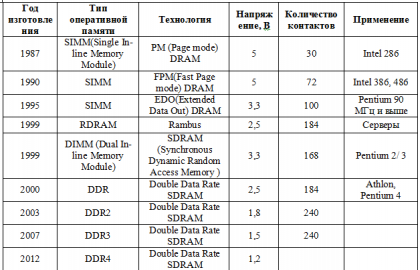
To begin with, we suggest that you familiarize yourself with the table, which presents the main parameters of RAM.
Types of DDR SDRAM memory modules
DDR SDRAM- twice the data rate of synchronous random access memory) - a type of RAM used in a PC. Thanks to DDR SDRAM, a greater bandwidth is achieved than with ordinary SDRAM, due to data transfer at the front and at the edge of the signal. This almost doubles the data transfer rate without increasing the memory bus frequency. Thus, when DDR operates at a frequency of 100 MHz, we will get an effective frequency of 200 MHz (when compared with the analogue SDR SDRAM).
In addition to transferring two data per clock, DDR SDRAM has several other fundamental differences from simple SDRAM memory. Basically they are technological. For example, a QDS signal has been added, which is located on the PCB along with the data lines. It is synchronized during data transfer. When using two memory modules, the data from them comes to the memory controller with a small time difference due to different distance to modules. This causes problems in choosing the clock signal for reading them, which the use of QDS successfully solves.
DDR SDRAM memory modules differ from SDRAM in the number of pins (184 pins for DDR modules versus 168 pins for modules with conventional SDRAM). At the same time, DDR modules operate at a supply voltage of 2.5 V, unlike SDRAM, which operates at 3.3 V, which significantly reduces heat dissipation.
DDR2 SDRAM modules
DDR2 SDRAM- double the data transfer rate of synchronous random access memory) - this type of RAM is currently the most common. DRR3 is noticeably more expensive, but this is just a matter of time, since DDR2 will be completely replaced in the near future.
Like DDR, DDR2 SDRAM uses data transfer on both slices of the clock signal, due to this, at the same memory bus frequency as in conventional SDRAM, you can actually double the data transfer rate (for example, when DDR2 operates at a frequency of 100 MHz, the effective frequency is obtained 200 MHz).
The main difference between DDR2 and DDR is twice the frequency of the bus, through which data is transferred to the buffer of the memory chip. At the same time, the operation of the microcircuit itself remained the same as in DDR (that is, with the same delays), but at a higher information transfer rate. DDR2 is not compatible with DDR, since the key is located in a different place on DDR2 modules compared to DDR, and it is impossible to insert a DDR2 module into the DDR socket without damaging the latter. Faster DDR2 modules are compatible with slower ones, while running at the frequency of the slowest module in the system. For PC use, DDR2 SDRAM comes in 240-pin DIMMs.
RAM type DDR3 SDRAM
DDR3 SDRAM- twice the data rate of synchronous random access memory) - this type of memory has a higher bandwidth. Reduces power consumption by 40% compared to DDR2 modules, using 90nm manufacturing technology, which allows lower operating currents and voltages (1.5V compared to 1.8V for DDR2 and 2.5V for DDR). "Dual-gate" transistors are also used to reduce leakage current, resulting in longer battery life in laptops. The improved design contributes to better cooling.
DDR4 SDRAM memory module
DDR4 SDRAM(double-data-rate three synchronous dynamic random access memory) - which differs from previous generations in higher frequency response and low voltage. Will support frequencies from 2133 to 4266 MHz. It is expected to go into mass production in 2012. January 4, 2011 at CES Samsung officially introduced new modules operating in DDR4-2133 mode at a voltage of 1.2 V.
Over the past ten years, computers have made a huge leap forward. During this time, many technologies managed to appear, gain popularity and become a thing of the past. Also with the development of RAM. In this article, we will consider all the main types of RAM that are used or have been used in personal computers.
any working memory modern computer refers to the DRAM or Dynamic random access memory type. It is volatile random access memory. This memory has two main characteristics: it is very fast and it is cleared when the power is turned off. That is why when you reboot, all unsaved data is lost, and turning on the computer takes so long. All necessary data must be read from and re-placed in memory.
Popular types of RAM
In turn, DRAM memory is divided into a large number of different types. Modern personal computers use these types of DRAM memory: DDR SDRAM, DDR2 SDRAM and DDR3 SDRAM.
All these three types of memory appeared in turn, each a new version received significant improvements over the previous one. They are not compatible with each other. Therefore, a computer equipped with a DDR memory slot cannot connect DDR2 memory, and so on.
To avoid erroneous installation of memory into a motherboard that is not suitable for it, memory modules have a different and incompatible shape. This can be seen in the picture above.
Form factors DIMM and SODIMM
Form factor (module design) for desktop computers is called a DIMM, and it is different from the form factor of laptop memory modules, which are called SODIMMs. This must be taken into account when for . Like desktop modules, DDR, DDR2, and DDR3 SODIMMs have design differences that prevent them from being installed in the wrong slot. See picture below.
Now all new computers are equipped with support exclusively for the most new memory DDR3 (in the form factor DIMM or SODIMM, depending on the type of computer). But, old versions of DDR and DDR2 can still be found on the market, so if you want to increase the amount of RAM in your old computer, this can be done without problems.
How to choose the right type of RAM
In order to expand the computer's RAM, you first need to find out what kind of memory it supports. This can be done in several ways:
- Unplug one RAM module and look at the sticker on it. The type of memory to which the given memory module belongs is always indicated there.
- Run one and z . With the help of such programs, you can always get all the necessary information about RAM and other components.
- But, if at the moment the computer is turned off and there are no RAM modules installed in it, you can get necessary information on the manufacturer's website.
Here, once again, I was asked how the type of RAM can be determined by appearance. Because such a question pops up from time to time, I decided that it’s better to show it once than to explain it on my fingers a hundred times, and write an illustrated mini-reviewer of RAM types for PC.
Not everyone is interested in this, so I hide it under the cat. Read
The most common types of RAM that have been used and are used in personal computers in everyday life are called SIMM, DIMM, DDR, DDR2, DDR3. You are unlikely to see SIMM and DIMM already, but DDR, DDR2 or DDR3 are now installed in most personal computers. So, in order
SIMM
SIMM for 30 contacts. They were used in personal computers with processors from 286 to 486. Now it is already a rarity. 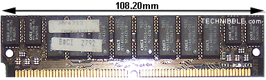 SIMM for 72 pins. Memory of this type was of two types FPM (Fast Page Mode) and EDO (Extended Data Out).
The FPM type was used on computers with 486 processors and in the first Pentiums until 1995. Then came EDO. Unlike its predecessors, EDO starts fetching the next block of memory at the same time it sends the previous block to the CPU.
Structurally, they are the same, you can only distinguish by marking. Personal computers that supported EDO could also work with FPM, but vice versa - not always.
DIMM
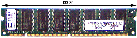
So called the type of memory SDRAM (Synchronous DRAM). Since 1996 most Intel chipsets began to support this type of memory module, making it very popular until 2001. Most computers with Pentium and Celeron processors used this type of memory.
DDR
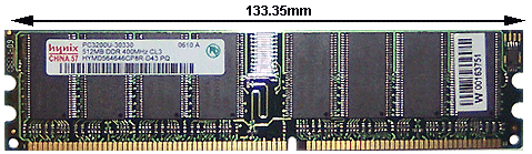 DDR (Double Data Rate) was the evolution of SDRAM. This kind of memory modules first appeared on the market in 2001. The main difference between DDR and SDRAM is that instead of doubling the clock speed to speed things up, these modules transfer data twice in one clock cycle.
DDR2
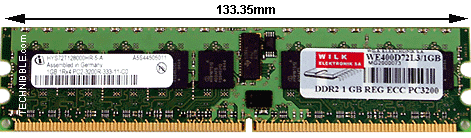
DDR2 (Double Data Rate 2) is a newer version of DDR that should theoretically be twice as fast. DDR2 memory first appeared in 2003, and the chipsets that support it - in mid-2004. The main difference between DDR2 and DDR is the ability to operate at a much higher clock frequency due to design improvements. In appearance, it differs from DDR in the number of contacts: it has increased from 184 (for DDR) to 240 (for DDR2).
DDR3
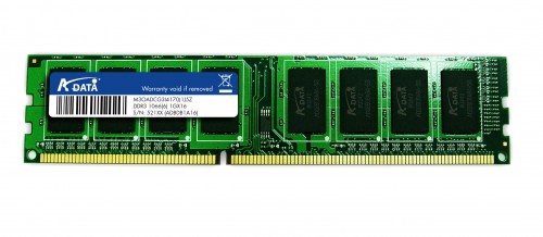 Like DDR2 memory modules, they are available in 240-pin printed circuit board(120 contacts on each side of the module), however, they are not electrically compatible with the latter, and for this reason they have a different location of the “key”.
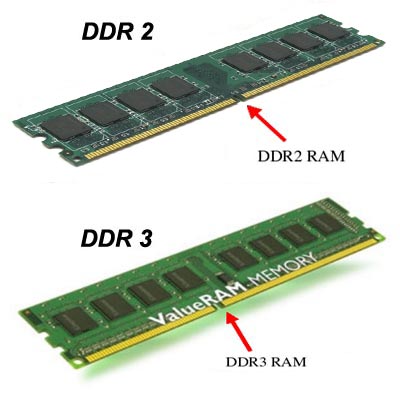
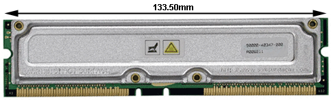
And finally, there is another type of RAM - RIMM (Rambus). Appeared on the market in 1999. It is based on traditional DRAM, but with a radically changed architecture. In personal computers, this type of RAM did not take root and was used very rarely. Such modules have been used in game consoles Sony Playstation 2 and Nintendo 64.
SIMM for 30 contacts.