In the previous section, we saw that DRAM chips multiplex addresses to save resources. We also saw that accessing DRAM cells takes time because the capacitors in these cells discharge in a way that does not immediately produce a stable signal. We also saw that DRAM cells need to be recharged. Now it's time to put it all together and see how these factors determine the details of DRAM access.
We will focus on modern technology, we will not discuss asynchronous DRAM and its variants as they are not relevant. Readers interested in this topic are referred to and. We also won't talk about Rambus DRAM (RDRAM), although this technology is not obsolete. It's just not widely used system memory. We will focus exclusively on synchronous DRAM (SDRAM - Synchronous DRAM) and its successor Double Data Rate DRAM (DDR).
Synchronous DRAM, as its name suggests, operates on a time source. The memory controller has a clock generator, the frequency of which determines the frequency of the system bus (FSB - Front Side Bus) - the memory controller interface used by DRAM chips. At the time of writing, frequencies of 800MHz, 1066MHz, and even 1333MHz are in use, with 1600MHz announced for the next generation. This does not mean that the bus frequency is really that high. Instead, data is transmitted two or four times in one clock cycle. Large numbers sells better, so manufacturers advertise a 200MHz bus with quadruple data rates as an 800MHz "effective" bus.
Today, for SDRAM, one piece of data transfer is 64 bits - 8 bytes. Therefore, the data transfer rate for the FSB is 8 bytes times the effective bus frequency (6.4Gb/s for a 200MHz bus with quadruple data transfer speed). This seems like a lot, but this is peak speed, a maximum that cannot be surpassed. As we will see, the communication protocol with the RAM module assumes that there are many periods of time when no data is transferred. These are precisely the periods of time that we must learn to understand and minimize in order to achieve the best performance.
2.2.1 Read access protocol
Figure 2.8: SDRAM read access protocol timing diagrams
Figure 2.8 shows the activity at some of the outputs of the DRAM module, which can be divided into three phases, which are colored differently in the figure. As usual, time flows from left to right. Many details are omitted. Here we are only talking about bus clocks, RAS and CAS signals, and address and data buses. The read cycle begins with the memory controller sending the row address along the address bus and lowering the RAS signal level. All signals are read while the clock signal (CLK) is rising, so it doesn't matter if the signals aren't exactly square waveforms - as long as they are stable when they start being read. Setting the row address causes the RAM chip to latch the address row.
The CAS signal can be sent over t RCD (RAS-to-CAS Delay) clock cycles. Then the column address is transmitted via the address bus and the CAS signal level is reduced. Here we see how two parts of an address (almost half) can be transmitted over the same address bus.
Finally, addressing is completed and data can be transferred. The RAM chip needs some time to prepare this. This delay is usually called CAS Latency (CL). In Figure 2.8 it is equal to 2. It can be higher or lower, depending on the quality of the memory controller, motherboard and DRAM module. It can also take half values. With CL=2.5, the first data will begin to be transmitted at the first drop in the clock signal in the blue region.
With all these preparations, it would be wasteful to transmit just one word of data. This is why DRAM modules allow the memory controller to set the amount of data transferred. Usually the choice is between 2, 4, or 8 words. This allows entire cache lines to be filled without a new RAS/CAS sequence. The memory controller can also send a CAS signal without a new row selection. This way, you can read or write sequential memory addresses much faster, due to the fact that you do not need to send a RAS signal and deactivate the line (see below). The memory controller must decide whether to keep the string "open". Theoretically, if you keep it open all the time, it could have negative consequences in existing applications(cm. ). When to send new signal CAS - determined by the Command Rate property of the RAM module (usually denoted as T x, Where x this value is such as 1 or 2, it will be 1 for high performance DRAM modules that accept new commands every cycle).
In this example, SDRAM outputs one word per cycle. This is what the first generation can do. DDR can transfer two words per cycle. This reduces transmission time but does not change latency. In principle, DDR2 works the same, although in practice it looks different. There is no need to go into detail here. Suffice it to note that DDR2 can be made faster, cheaper, more reliable and more energy efficient (see for more details).
2.2.2 Pre-charge and activation
Figure 2.8 does not cover the full cycle. It shows only part of the complete DRAM access cycle. Before a new RAS signal can be sent, the currently selected line must be deactivated and the new line must be charged. We can concentrate here on the case where this is done by an explicit command. There are protocol improvements that, in some cases, eliminate this extra step. However, the delay caused by charging still affects the operation.

Figure 2.9: SDRAM Precharge and Activation
Figure 2.9 shows activity starting from one CAS signal and ending with a CAS signal for another line. The data requested by the first CAS signal appears as before through CL cycles. This example requires two words that take two cycles to transfer to SDRAM. You can imagine four words on a DDR chip.
Even on DRAM modules with a command rate of 1, the precharge command cannot be issued immediately. You must wait while the data is being transmitted. In our case, these are two cycles. It turns out the same as CL, but that's just a coincidence. The precharge signal does not have a special dedicated line. Instead, some implementations use lower Write Enable (WE) and RAS levels simultaneously. This combination has no meaning on its own (see coding details in ).
Once the precharge command is issued, t RP (Row Precharge time) cycles must be waited before the row can be selected. In Figure 2.9, most of this time (in purple) overlaps with data transfer (in light blue). This is good! But t RP is longer than the data transfer time, so the next RAS signal is delayed by one cycle.
If we were to continue the time axis in the diagram, we would find that the next data transfer begins 5 cycles after the end of the current one. This means that the data bus is used in only two cycles out of seven. Multiply that by the FSB speed, and the theoretical 6.4Gb/s on an 800MHz bus becomes 1.8Gb/s. This is bad and should be avoided. The techniques described in Chapter 6 will help you increase this speed. But the programmer must try for this.
There is one more timing constant for SDRAM modules that we haven't discussed. In Figure 2.9, the precharge command is limited only by the data transmission time. Another limitation is that the SDRAM module needs time after the RAS signal before it can charge another row (this time is denoted tRAS). This number is usually quite high, two or three times the tRP value. This is a problem if the RAS signal is followed by only one CAS signal and the data transfer ends after several cycles. In Figure 2.9, assume that the first CAS signal is immediately preceded by a RAS signal and t RAS is equal to 8 cycles. Then the precharge command must be delayed by one cycle, since the sum of t RCD , CL, and t RP (since it is greater than the data transfer time) is only 7 cycles.
DDR modules are often described using a special notation: w-x-y-z-T. For example: 2-3-2-8-T1. It means:
w 2 CAS Latency (CL) x 3 RAS -to-CAS delay (t RCD ) y 2 RAS Precharge(tRP) z 8 Active to Precharge delay (t RAS) T T1 Command Rate
There are many more time constants that affect how commands should be issued and executed. But in practice, these five constants are enough to determine the performance of the module.
Sometimes it is useful to know this information about the computer you are using in order to correctly interpret certain measurements. And it's definitely useful to know these details when you're buying a computer, as they, along with FSB and SDRAM speeds, are some of the most important factors that determine a computer's performance.
The adventurous reader may also try to customize the system. Sometimes the BIOS allows you to change some or all of these values. SDRAM modules have programmable registers where these values can be set. Typically the BIOS will choose the best default value. If the RAM module High Quality, then it may be possible to reduce one of the delays without affecting the stability of the computer. Numerous overclocking sites on the Internet offer a ton of documentation about this. Do this at your own peril and risk, but don’t say later that you weren’t warned.
2.2.3 Reloading
The most commonly overlooked topic when considering DRAM access is recharging. As shown in Section 2.1.2, DRAM cells need to be constantly refreshed. And this does not happen unnoticed by the rest of the system. When a string is overcharged (the unit of measurement here is string (see), although other literature states otherwise), it cannot be accessed. The study shows that "surprisingly, DRAM recharging can have a dramatic impact on performance."
According to the JEDEC (Joint Electron Device Engineering Council) specification, each DRAM cell must be recharged every 64ms. If the DRAM array has 8192 rows, this means that the memory controller must send a recharge command on average every 7.8125 microseconds (these commands may be queued and so in practice the maximum interval between two of them may be greater). It is the responsibility of the memory controller to manage the schedule of recharge commands. The DRAM module remembers the address of the last reloaded row and automatically increments the address counter for each new instruction.
The programmer has little influence on recharging and the timing at which these commands are given. But it's important to have this part life cycle DRAM is in mind when interpreting measurements. If an important word needs to be read from a string, and the string is being recharged at that moment, the processor may be idle for quite a long time. How long charging takes depends on the DRAM module.
2.2.4 Memory types
It is worth spending a little time describing the existing memory types and their closest successors. We'll start with SDR (Single Data Rate) SDRAM, since they are the basis for DDR (Double Data Rate) SDRAM. SDRs were very simple. The speed of memory cells and data transfer was the same.
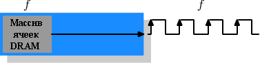
Figure 2.10: SDR SDRAM Operations
In Figure 2.10, a DRAM memory cell can output memory contents at the same rate as it is transported across the memory bus. If a DRAM cell can operate at 100 MHz, then the bus data transfer rate will be 100 MB/s. Frequency f is the same for all components. Raise throughput DRAM chip is expensive because power consumption increases with frequency. Given the huge number of cell arrays, this is impossibly expensive. ( Power Consumption = Dynamic Capacitance × Voltage 2 × Frequency). In fact, this is an even bigger problem, since increasing the frequency also requires increasing the voltage to maintain system stability. In DDR SDRAM (later called DDR1), bandwidth was increased without increasing any of the frequencies involved.

Figure 2.11: DDR1 SDRAM Operations
The difference between SDR and DDR1, as can be seen in Figure 2.11 and understood from the name, is that double the amount of data is transferred in one cycle. That is, the DDR1 chip can transmit data as the signal level increases and decreases. This is sometimes called a "double pump" tire. To make this possible without increasing the frequency of the memory cell array, a buffer is used. The buffer stores two bits per data line. This, in turn, requires that the cell array in Figure 2.7 have a two-line data bus. The implementation of this is trivial: you need to use the same column address for two DRAM cells and access them in parallel. Changes to the cell array will be minimal.
SDR DRAMs were known simply by their frequency (eg PC100 for 100MHz SDR). To improve the sound of DDR1 DRAM, marketers had to change this circuit, since the frequency did not change. They adopted a name that contains the byte rate that the DDR module supports (it has a 64-bit wide bus):
100MHz × 64bit × 2 = 1600Mb/s
Hence, the 100MHz DDR module is called PC1600. With 1600 > 100 all marketing requirements are met - it sounds much better, although the real improvement is only twofold. ( I would understand if they doubled it, otherwise the numbers would be inflated.}

Figure 2.12: DDR2 SDRAM Operations
To get even more out of the technology, DDR2 includes a few more innovations. The most obvious change, as can be seen from Figure 2.1, is the doubling of the bus frequency. Doubling the frequency means doubling the throughput. Since doubling the frequency is not economically feasible for a cell array, the I/O buffer is now required to receive four bits per cycle, which it then transfers across the bus. This means that the changes to the DDR2 module are to increase the speed of the DIMM I/O buffer. It's definitely possible and doesn't require significantly more power - it's just one small component, not the entire module. The name that marketers came up with for DDR2 is similar to the name for DDR1, only in calculating the value the multiplier of two is replaced by four (now we have a “quadruple pumping” bus). Figure 2.13 shows the module names used today.
Frequency
arrayFrequency
tiresSpeed
dataName
(speed)Name
(FSB)133MHz 266MHz 4256Mb/s PC2-4200 DDR2-533 166MHz 333MHz 5312Mb/s PC2-5300 DDR2-667 200MHz 400MHz 6400Mb/s PC2-6400 DDR2-800 250MHz 500MHz 8000Mb/s PC2-8000 DDR2-1000 266MHz 533MHz 8512Mb/s PC2-8500 DDR2-1066 Figure 2.13: DDR2 module names
There's another trick in the name. FSB speed used by CPU motherboard and by the DRAM module is expressed in terms of the “effective” frequency. That is, it is multiplied by 2 due to the fact that data transmission occurs as the signal level of the clock generator increases and decreases and the number increases. So, a 133MHz module with a 266MHz bus has a FSB “frequency” of 533MHz.
DDR3 specification (the real one, not the GDDR3 used in graphic cards) implies further changes that continue the logic of the transition to DDR2. The voltage will be reduced from 1.8V for DDR2 to 1.5V for DDR3. Since power consumption is proportional to the square of the voltage, this alone gives a 30% improvement. Add in chip reduction and other electrical improvements, and DDR3 can consume half the power at the same frequency. And at a higher frequency you can get by with the same amount. Or you can double the capacity for the same amount of heat output.
The DDR3 module's cell array will run at a quarter of the external bus speed, requiring an eight-bit I/O buffer, up from DDR2's four-bit. Figure 2.14 shows the diagram.
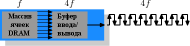
Figure 2.14: DDR3 SDRAM Operations
It's likely that DDR3 modules will initially have slightly higher CAS latency than DDR2 because DDR2 is a more mature technology. Therefore, using DDR3 will only make sense at higher frequencies than those achievable by DDR2, or when throughput is more important than latency. There is already talk about 1.3V modules that will have the same CAS latency as DDR2. In any case, the opportunity to achieve more high speeds due to faster buses will outweigh the increase in latency.
One possible problem with DDR3 is that at speeds of 1600Mb/s and higher, the number of modules per channel can be reduced to one. IN earlier versions this limitation was present for all frequencies, so it is hoped that over time it will be removed for all frequencies. Otherwise, the capacity of the systems will be severely limited.
Figure 2.15 shows the expected DDR3 module names. JEDEC had by this time approved the first four types. Considering that Intel's 45nm processors have a FSB speed of 1600Mb/s, it is necessary to have 1866Mb/s for the overclocker market. We'll likely see this towards the end of DDR3's life cycle.
Frequency
arrayFrequency
tiresSpeed
dataName
(speed)Name
(FSB)100MHz 400MHz 6400Mb/s PC3-6400 DDR3-800 133MHz 533MHz 8512Mb/s PC3-8500 DDR3-1066 166MHz 667MHz 10667Mb/s PC3-10667 DDR3-1333 200MHz 800MHz 12800Mb/s PC3-12800 DDR3-1600 233MHz 933MHz 14933Mb/s PC3-14900 DDR3-1866 Figure 2.15: DDR3 module names
All DDR memory has one problem - increasing the bus frequency makes it difficult to create parallel data buses. The DDR2 module has 240 pins. All connections to the data and address pins should be made so that they are approximately the same length. Even more problematic is that when there are multiple DDR modules on the same bus, the signals become more and more distorted for each additional module. The DDR2 specification allows the use of only two modules on one bus (channel), DDR3 - only one module at high frequencies. With 240 pins per channel, a single Northbridge cannot handle more than two channels well. An alternative is to use external memory controllers (see Figure 2.2), but this is very expensive.
All this means is that motherboards mass computers can have no more than four DDR2 or DDR3 modules. This severely limits the amount of memory the system can have. Even the old 32-bit IA-32 processors supported up to 64GB of RAM, and the need for large amounts of memory is growing even for home systems, so something needs to be done.
One solution is to add memory controllers to each processor, as shown at the beginning of this chapter. AMD is doing this with the Opteron line of processors, and Intel will be doing this with CSI technology. This can help as long as the amount of memory the processor is capable of using can be attached to each processor. In some situations this is not the case and this approach leads to the NUMA architecture with its negative effects. For some situations, a completely different solution is needed.
Intel's solution for large server machines, at least for the coming years, is called Fully Buffered DRAM (FB-DRAM). FB-DRAM modules use the same components as today's DDR2 modules, making them relatively cheap to manufacture. The difference is the connection to the memory controller. Instead of a parallel data bus, FB-DRAM uses a serial bus (the same was true for Rambus DRAM and SATA, a successor to PATA, and PCI Express after PCI/AGP). The serial bus can be driven at a much higher frequency, overcoming the negative effects of serialization, and even increasing throughput. The main effects of using a serial bus:
- you can use more modules on one channel,
- more channels can be used on one Northbridge/memory controller,
- The serial bus is full duplex (two lines).
The FB-DRAM module has only 69 pins, instead of 240 for DDR2. Using multiple FB-DRAM modules together is much easier because the electrical effects of such a bus are easier to control. The FB-DRAM specification allows the use of up to 8 modules per channel.
Given the interconnection requirements of a dual-channel Northbridge, it is now possible to drive six FB-DRAM channels with fewer pins: 2x240 versus 6x69. The on-board path to each channel is also much simpler, which can help keep the price of motherboards down.
Full duplex parallel buses are too expensive for traditional DRAM modules - it is very expensive to double the number of lines. With serial lines (even if they are differential as required by FB-DRAM) this is not the case, so the serial bus is made fully duplex, which means in some situations that the bandwidth is doubled just because of this. But this is not the only case where parallelism is used to increase throughput. Since the FB-DRAM controller can handle up to six channels simultaneously, throughput using FB-DRAM can be increased even for systems with a small amount of RAM. Where a DDR2 system with four modules has two channels, the same capacity can be served through four channels by a conventional FB-DRAM controller. Actual serial bus bandwidth depends on which DDR2 (or DDR3) chips are used in the FB-DRAM modules.
We can summarize the benefits this way:
There are downsides to FB-DRAM when using multiple DIMMs on the same channel. The signal is delayed, although only minimally for each DIMM in the chain, which means increased latency. But for the same amount of memory at the same frequency, FB-DRAM will always be faster than DDR2 and DDR3, since only one DIMM is needed per channel. For systems with large amounts of memory, DDR simply does not have a solution on mass components.
2.2.5 Conclusions
This section was meant to show that accessing DRAM cannot be an arbitrarily fast process. At least compared to processor speed and processor access speed to registers and cache. It is important to keep in mind the differences between CPU and memory frequencies. CPU Intel Core 2 is clocked at 2.933 GHz, and the front side bus at 1.066 GHz will have a clock ratio of 11:1 (note that the bus runs at four times the bus speed). An idle time of one memory cycle means an idle time of 11 processor cycles. Most machines actually use slower DRAM, which further increases latency. Keep these numbers in mind when we talk about downtime in later chapters.
The read command graphs show that DRAM modules are capable of transferring data at a fast and sustained rate. Entire lines of DRAM can be transferred without a single delay. The data bus can remain 100% busy. For DDR modules, this means that two 64-bit words are transferred each cycle. For DDR2-800 modules on two channels this is 12.8Gb/s.
But access to DRAM is not always sequential, unless of course it is specifically organized that way. Distant memory locations are used, which means that pre-charging and new RAS signals are unavoidable. That's when things slow down and the DRAM modules need help. The sooner precharge occurs and the RAS signal is sent, the lower the cost of using a new line.
To reduce downtime and create more time overlap between their callers, hardware and software prefetching is used (see Section 6.3). It also helps move memory operations in time so that fewer resources are needed later, before the data is needed. A problem that often arises is that data produced in one round needs to be stored, but data needed in the next round needs to be read. By moving reading in time, we will ensure that read and write operations do not need to be done simultaneously.
- Faster, even faster, please speed up, at least a little, otherwise I’ll be…
– I can’t, dear Gamer, because I’ve reached my maximum clock frequency.
The dialogue of a Gamer, for whom every fraction of a second counts, could look something like this.
Clock frequency random access memory(RAM, RAM) is the second most important parameter after volume. The higher it is, the faster the data exchange between the processor and RAM occurs, the faster the computer works. RAM with low clock rates can become a bottleneck in resource-intensive games and programs. And if you don’t want to ask the capricious piece of hardware to speed up a little every time, always pay attention to this characteristic when purchasing. Today we’ll talk about how to find out the frequency of RAM based on the description in store catalogs, as well as the one installed on your PC.
How to understand what kind of “beast” a store offers
In the description of RAM modules on online store websites, sometimes not all of them are indicated, but only certain speed characteristics. For example:- DDR3, 12800 Mb/s.
- DDR3, PC12800.
- DDR3, 800 MHz (1600 MHz).
- DDR3, 1600 MHz.
Some might think that in this example we are talking about four different planks. In fact, this can be used to describe the same RAM module with an effective frequency of 1600 MHz! And all these numbers indirectly or directly point to it.
To avoid any further confusion, let’s figure out what they mean:
- 12800 Mb/s is the memory bandwidth, an indicator obtained by multiplying the effective frequency (1600 MHz) by the bus width of one channel (64 bits or 8 bytes). Bandwidth describes the maximum amount of information that a RAM module is capable of transmitting in one clock cycle. I think it’s clear how to determine the effective frequency from it: you need to divide 12800 by 8.
- PC12800 or PC3-12800– another designation for the throughput of a RAM module. By the way, a set of two strips intended for use in dual-channel mode has 2 times higher bandwidth, so its label may indicate PC25600 or PC3-25600.
- 800 MHz (1600 MHz)– two values, the first of which indicates the frequency of the memory bus itself, and the second - 2 times larger - its effective frequency. How are the indicators different? Computers, as you know, use DDR type RAM - with double the data transfer rate without increasing the number of bus cycles, that is, in 1 clock cycle not one, but two conventional pieces of information are transmitted through it. Therefore, the main indicator is considered to be effective clock frequency(in this example – 1600 MHz).
The screenshot below shows a description of the speed characteristics of the RAM from the catalogs of three computer stores. As you can see, all sellers designate them differently.

Different RAM modules within the same generation - DDR, DDR2, DDR3 or DDR4 - have different frequency characteristics. Thus, the most common DDR3 RAM in 2017 is available with frequencies of 800, 1066, 1333, 1600, 1866, 2133 and 2400 MHz. Sometimes it is designated as such: DDR3-1333, DDR3-1866, etc. And this is convenient.
Not only the RAM has its own effective frequency, but also the device that controls it - the memory controller. In modern computer systems, starting from generation Sandy Bridge, it is part of the processor. In older ones - as part of the components north bridge motherboard.
Almost all RAM can operate at lower clock speeds than specified in the specifications. RAM modules with different frequencies, provided that other parameters are similar, are compatible with each other, but can only function in single-channel mode.
If the computer has several RAM sticks with different frequency characteristics, the memory subsystem will exchange data at the speed of the slowest link (with the exception of devices). So, if the controller frequency is 1333 MHz, one of the strips is 1066 MHz, and the other is 1600 MHz, the transmission will proceed at a speed of 1066 MHz.
How to find out the frequency of RAM on a computer
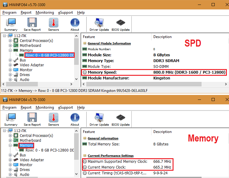
Before learning how to determine the frequency indicators of RAM on a PC, let’s figure out how the computer itself recognizes them. It reads the information recorded in the SPD chip, which is equipped with each individual RAM stick. What this microcircuit looks like is shown in the photo below.
SPD data can also be read by programs, for example, the well-known utility, one of the sections of which is called “ SPD" In the screenshot below we see the already familiar characteristics of the speed of the RAM strip (field “ MaxBandwidth") - PC3-12800 (800 MHz). To find out its effective frequency, just divide 12800 by 8 or multiply 800 by 2. In my example, this figure is 1600 MHz.
However, in CPU-Z there is another section - “ Memory", and in it - the parameter " DRAMFrequency", equal to 665.1 MHz. This, as you probably guessed, is actual data, that is, the frequency mode in which the RAM actually operates. If we multiply 665.1 by 2, we get 1330.2 MHz - a value close to 1333 - the frequency at which the memory controller of this laptop operates.

In addition to CPU-Z, similar data is shown by other applications used to recognize and monitor PC hardware. Below are screenshots of the free utility:
Other options identical in purpose: Memory Frequency, DRAM Clock By, MEM Clock Setting, Memory Clock (Mhz), New MEM Speed (DDR), System Memory Frequency.
The DRAM Frequency option is one of the most commonly used BIOS options related to configuring the operation of the computer's RAM. It allows the user to set one of the most important RAM parameters – the operating frequency of the memory chips.
RAM is one of the most important components personal computer. Its purpose is to store data that is used operating system and application programs during the current work session. At the hardware level, RAM is made in the form of special modules on which microcircuits are located that contain the actual information storage cells. These modules are inserted into special expansion slots on motherboard.
Typically, computer RAM falls into the category of dynamic memory. Dynamic memory () is distinguished from static memory by lower performance, but also more low price. Another feature of dynamic memory is its need for dynamic updating of data in the microcircuits installed on it.
Currently, modules made using DDR (Double Data Rate) Synchronous DRAM technology are used for RAM. DDR modules use synchronous, that is, clock-determined, operating mode, and have twice the bandwidth compared to conventional synchronous memory modules (SDRAM).
The operating frequency of dynamic RAM can be considered one of the most important parameters of its operation, since it largely determines its performance. Typically, memory frequency refers to the frequency of the memory bus on the motherboard.
It is necessary to distinguish the real frequency of the memory bus, which means the number of pulses created by the clock generator, from the effective one. The effective frequency is, in fact, the real speed of operations performed during memory operation, and for modern types RAM modules, such as DDR2 and DDR3, can be several times higher than the real one.
DDR RAM modules, as a rule, operate at frequencies of 200, 266, 333, 400 MHz. DDR2 modules usually have twice the effective frequency characteristics compared to DDR2 - 400, 533, 667, 800, 1066 MHz, and, therefore, twice the performance. DDR3 memory, in turn, has twice the effective frequency compared to DDR2 - 800, 1066, 1333, 1600, 1800, 2000, 2133, 2200, 2400 MHz.
To set the operating frequency of RAM modules, many BIOS have a DRAM Frequency function, as well as similar options.
These options are usually found only on those motherboards that have RAM controllers that allow it to operate in asynchronous modes, that is, at frequencies independent of the system bus frequency. Since memory controllers in modern motherboards are usually built into the chipset, chipsets with such controllers are called asynchronous. Motherboards with asynchronous chipsets provide the user with ample opportunities for overclocking RAM.
The DRAM Frequency option may have various options values. The Auto value means that the RAM speed is determined automatically by the BIOS. The value by SPD means that the operating frequency is determined by special chips built into memory modules - SPD (Serial Presence Detect) chips.
Also, this option often allows you to select exact RAM frequency values from a specific set of values supported by the motherboard. These values are always indicated in megahertz.
In some BIOS you may also find options like 1:1, Linked, Host Clk. These options imply setting the operating frequency of the memory modules equal to the operating frequency of the system bus.
Which option should I choose?
For most users, it is best to set it to Auto so that the BIOS can automatically select the optimal value. However, sometimes it happens that the BIOS can set a frequency lower than that which is rated for the RAM. To fix this, you can set the option to by SPD or manually select the required frequency value option.
Also manual installation Memory frequencies are often used when overclocking a computer. As you know, increasing the frequency of RAM in most cases improves computer performance, although not to such a large extent as increasing the speed of the processor. Typically, the performance gain when overclocking RAM can range from 4 to 12%. In addition to targeted overclocking of a specific PC component, there are options such as those that can handle complex overclocking.
To overclock the memory, the user can specify the required frequency value in the option, and then test its operation using special test programs. If the RAM operates without errors, the set value can be left as a constant.
However, it is not only setting the RAM frequency that is too high that can have negative consequences. In some cases, setting values that are too low, beyond the specifications of the RAM modules, can also lead to errors, including errors during booting of the computer.
Operating principle
How DRAM Read Works for a Simple 4x4 Array

How DRAM Write Works for a Simple 4x4 Array
Physically, DRAM memory is a collection of storage cells that consist of capacitors and transistors located inside semiconductor memory chips.
Initially, memory chips were produced in DIP-type packages (for example, the K565RUxx series), then they began to be produced in more technologically advanced packages for use in modules.
Many SIMM modules and the vast majority of DIMMs had SPD (Serial Presence Detect) installed - a small EEPROM memory chip that stores module parameters (capacity, type, operating voltage, number of banks, access time, etc.), which were available in software as hardware , in which the module was installed (used for auto-configuring parameters), and to users and manufacturers.
SIPP modules
SIPP (Single In-line Pin Package) type modules are rectangular boards with contacts in the form of a series of small pins. This type of design is practically no longer used, since it was later replaced by SIMM-type modules.
SIMM modules
SIMM (Single In-line Memory Module) type modules are long rectangular boards with a number of pads along one of its sides. The modules are fixed in the connection connector (socket) using latches, by installing the board at a certain angle and pressing it until it is brought to a vertical position. Modules of 4, 8, 16, 32, 64, 128 MB were produced.
The most common are 30- and 72-pin SIMMs.
DIMMs
Modules of the DIMM type (Dual In-line Memory Module) are long rectangular boards with rows of contact pads along both sides, installed vertically into the connection connector and secured at both ends with latches. Memory chips on them can be placed on one or both sides of the board.
SDRAM memory modules are most common in the form of 168-pin DIMM modules, DDR SDRAM memory modules are in the form of 184-pin modules, and DDR2, DDR3 and FB-DIMM SDRAM memory modules are 240-pin modules.
SO-DIMMs
For portable and compact devices (Mini-ITX form factor motherboards, laptops, notebooks, tablets, etc.), as well as printers, network and telecommunications equipment, etc., structurally reduced DRAM modules (both SDRAM and DDR SDRAM) - SO-DIMM (Small outline DIMM) - analogues of DIMM modules in a compact design to save space.
SO-DIMMs are available in 72-, 100-, 144-, 200-, and 204-pin versions.
RIMM modules
Modules of the RIMM type (Rambus In-line Memory Module) are less common; they come with RDRAM type memory. They are represented by 168- and 184-pin varieties, and on the motherboard such modules must be installed only in pairs, otherwise special plug modules are installed in empty connectors (this is due to the design features of such modules). There are also 242-pin PC1066 RDRAM RIMM 4200 modules, which are not compatible with 184-pin connectors, and a smaller version of RIMM - SO-RIMM, which are used in portable devices.
Chip manufacturers and module assemblers
Top five largest producers According to the results of the first quarter of 2008, DRAM included