Intel Pentium processor family
- P54CS
- Tillamook
Pentium(pronounced Pentium) - trademark several generations of microprocessors of the x86 family, manufactured by Intel Corporation since March 22, 1993. The Pentium is Intel's fifth-generation processor and replaces the Intel 80486 (often referred to simply as the 486).
Story
Models
Initially (March 22, 1993), only two models were presented, based on the P5 core with frequencies of 60 and 66 MHz. Later, more powerful Pentium processors were released, based on improved cores. In addition, they were presented mobile versions processors and Pentium OverDrive processors.
| Kernel codename | P5 | P54C | P54CS | P55C | |||||||||
|---|---|---|---|---|---|---|---|---|---|---|---|---|---|
| Technical process, nm | 800 | 600 | 350 | ||||||||||
| Core clock frequency, MHz | 60 | 66 | 75 | 90 | 100 | 120 | 133 | 150 | 166 | 200 | 166 | 200 | 233 |
| Announced | March 23, 1993 | October 10, 1993 | March 7, 1994 | March 27, 1995 | June 12, 1995 | January 4, 1996 | June 10, 1996 | January 8, 1997 | June 2, 1997 | ||||
P5
The only two models of first-generation Pentium processors, with core clock speeds of 60 and 66 MHz, were announced on March 23, 1993.
The processor was produced in a 273-pin CPGA package, was installed on the motherboard in the Socket 4 processor socket and required a 5 V power supply. The system bus (FSB) frequency was equal to the core frequency, that is, the core multiplier was equal to 1.0.
All Pentium processors belong to the SL Enhanced class - this means that they have an SMM system that reduces power consumption. The second level cache was located on motherboard and could be up to 1 MB in size. Early versions of processors, with frequencies of 60-100 MHz (P5 and P54C cores), had a bug in the math coprocessor module, which in rare cases led to a decrease in the accuracy of the division operation. This defect was discovered in 1994 and became known as the "Pentium FDIV bug".
Processors based on the P5 core were manufactured using an 800-nanometer process technology using bipolar BiCMOS technology. The processor contains 3.1 million transistors, and the core die size is 294 mm². The Pentium 66 consumes a current of 3.2 A and has a power of 16 W, which required the installation of an additional fan. The production of such processors turned out to be very difficult and the percentage of usable crystals turned out to be too small. Many experts, pointing out the numerous shortcomings (see: F0 0f c7 c8) of the first generation Pentium processors, did not advise buying these models. Production had to be stopped for a while. However, production of improved processors based on the P54C core soon began.
P54C
Second generation Pentium processors use multiplication clock frequency, it runs faster than the system bus. A multiplier is used to indicate how many times the processor core clock frequency is greater than the system bus frequency. In all processors based on the P54C core, the multiplier is 1.5.
P54CS
The first processors based on this core were released on March 27, 1995. In essence, this core is a P54C core manufactured using 350 nm bipolar BiCMOS technology, which made it possible to reduce the core die size to 91 mm² (Pentium 120 and 133 processors), but soon, as a result of core optimization, its size was reduced up to 83 mm² with the same number of transistors. At the same time, the Pentium 200 consumed a current of 4.6 A, and its maximum energy dissipation (heat dissipation) was 15.5 W.
P55C
On January 8, 1997, Pentium processors based on the third generation P5 core (P55C) were released. The Intel R&D Center in Haifa (Israel) added a new set of instructions to the P55C core, called MMX (MultiMedia eXtension), which significantly increases (from 10 to 60%, depending on optimization) computer performance in multimedia applications. As a result, these processors are called Pentium w/MMX technology (usually shortened to Pentium MMX). The new processor includes an MMX device with pipelined instruction processing, the L1 cache is increased to 32 KB (16 KB for data and 16 KB for instructions). Consists of new processor of 4.5 million transistors and is produced using advanced 280-nanometer CMOS technology using silicon semiconductors, operates at a voltage of 2.8 V. The maximum current consumption is 6.5 A, heat dissipation is 17 W (for Pentium 233 MMX). The crystal area of Pentium MMX processors is 141 mm². The processors were produced in a 296-pin CPGA or PPGA package for Socket 7.
Pentium OverDrive
Several generations of Pentium OverDrive were released.
- In 1995, the first Pentium OverDrive was released (on the P24T core). It was designed for installation in Socket 2 or Socket 3 sockets and worked with a supply voltage of 5 V, that is, it was used for upgrading systems using a 486 processor without replacing the motherboard. Moreover, this processor had all the functions of the first generation Pentium processor (on the P5 core). Two models were released, operating at frequencies of 63 and 83 MHz, the older one consumed a current of 2.8 A and had a power dissipation of 14 W. Due to the high cost, this processor left before it appeared. And although after some time (March 4, 1996) these processors were replaced by Pentium ODP5V with frequencies of 120 and 133 MHz, based on the P5T core (essentially a P54CS core), they also did not become popular.
- On March 4, 1996, the next version of Pentium OverDrive was released - Pentium ODP3V - based on the P54CT core. This core is based on the P54CS core. The processor was produced in a 320-pin CPGA package for Socket 5 or Socket 7.
- On March 3, 1997, two Pentium ODPMT models were released (with frequencies of 150 and 166 MHz), built on the P54CTB core (analogous to the P55C). Later, on August 4, 1997, two more models were released on the same core (with frequencies of 180 and 200 MHz). They were produced in 320-pin CPGA packages and were designed for Socket 5 or Socket 7 (Pentium ODPMT-200 MMX - Socket 7 only).
Tillamook
Processors based on this core were intended for laptop computers and were used in the so-called. "mobile module" MMC-1 Mobile Module Connector with 280 pins worked together with Intel chipset 430 TX and having 512 KB of cache memory on system board. The Tillamook core (named after a city in Oregon, USA) is a lower-voltage P55C core - the 300 MHz model operated at 2.0 V, consuming 4.5 A, and dissipating 8 ,4 W. Older models (with a frequency of 233, 266 and 300 MHz) were produced using a 250 nm process technology and had a crystal area of 90 mm²; there were also versions with a 166 MHz core frequency. Models 200 and 233 were produced from August 1997, model 266 from January 1998 , and the top model in the line was introduced in January 1999.
(which is often called simply 486).
Encyclopedic YouTube
1 / 4
Why Were Pentium 2"s on Cards? | Nostalgia Nerd
Pentium vs 486 PC (1993)
Armado y desarmado de un CPU Pentium 4, práctica de un estudiante en informática.
Why Pentium Kicks 486 Ass (Pipelines & Cache) | Nostalgia Nerd
Subtitles
Story
Processors based on the P5 core were manufactured using an 800-nanometer process technology using bipolar BiCMOS technology. The processor contains 3.1 million transistors, and the core die size is 294 mm². The Pentium 66 consumes a current of 3.2 A and has a power of 16 W, which required the installation of an additional fan. The production of such processors turned out to be very difficult and the percentage of usable crystals turned out to be too small. Many experts, pointing out the numerous shortcomings (see: F0 0f c7 c8) of the first generation Pentium processors, did not advise buying these models. Production had to be stopped for a while. However, production of improved processors based on the P54C core soon began.
P54C
The second generation Pentium processors use clock multiplication and are faster than the system bus. A multiplier is used to indicate how many times the processor core clock frequency is greater than the system bus frequency. In all processors based on the P54C core, the multiplier is 1.5.
P54CS
The first processors based on this core were released on March 27, 1995. In essence, this core is a P54C core manufactured using 350 nm bipolar BiCMOS technology, which made it possible to reduce the core die size to 91 mm² (Pentium 120 and 133 processors), but soon, as a result of core optimization, its size was reduced up to 83 mm² with the same number of transistors. At the same time, the Pentium 200 consumed a current of 4.6 A, and its maximum energy dissipation (heat dissipation) was 15.5 W.
P55C
On January 8, 1997, Pentium processors based on the third generation P5 core (P55C) were released. The Intel R&D Center in Haifa (Israel) added a new set of instructions to the P55C core, called MMX (MultiMedia eXtension), which significantly increases (from 10 to 60%, depending on optimization) computer performance in multimedia applications. As a result, these processors are called Pentium w/MMX technology (usually shortened to Pentium MMX). The new processor includes an MMX device with pipelined instruction processing, the L1 cache is increased to 32 KB (16 KB for data and 16 KB for instructions). The new processor consists of 4.5 million transistors and is manufactured using advanced 280-nanometer CMOS technology using silicon semiconductors, operates at a voltage of 2.8 V. The maximum current consumption is 6.5 A, heat dissipation is 17 W (for Pentium 233 MMX ). The crystal area of Pentium MMX processors is 141 mm². The processors were produced in a 296-pin CPGA or PPGA package for Socket 7.
Pentium OverDrive
Several generations of Pentium OverDrive were released.
- In 1995, the first Pentium OverDrive was released (on the P24T core). It was designed for installation in Socket 2 or Socket 3 type sockets and worked with a supply voltage of 5 V, that is, it was used for upgrading systems using the 486 processor without replacing the motherboard. Moreover, this processor had all the functions of the first generation Pentium processor (on the P5 core). Two models were released, operating at frequencies of 63 and 83 MHz, the older one consumed a current of 2.8 A and had a power dissipation of 14 W. Due to the high cost, this processor left before it appeared. And although after some time (March 4, 1996) these processors were replaced by Pentium ODP5V with frequencies of 120 and 133 MHz, based on the P5T core (essentially a P54CS core), they also did not become popular.
- On March 4, 1996, the next version of Pentium OverDrive was released - Pentium ODP3V - based on the P54CT core. This core is based on the P54CS core. The processor was produced in a 320-pin CPGA package for Socket 5 or Socket 7.
- On March 3, 1997, two Pentium ODPMT models (with frequencies of 150 and 166 MHz), built on the P54CTB core (analogous to the P55C), were released. Later, on August 4, 1997, two more models were released on the same core (with frequencies of 180 and 200 MHz). They were produced in 320-pin CPGA packages and were designed for Socket 5 or Socket 7 (Pentium ODPMT-200 MMX - Socket 7 only).
Tillamook
Processors based on this core were intended for laptop computers and were used in the so-called. The "mobile module" MMC-1 Mobile Module Connector with 280 pins worked together with the Intel 430 TX chipset and had 512 KB of cache memory on the motherboard. The Tillamook core (named after a city in Oregon, USA) is a lower-voltage P55C core - the 300 MHz model operated at 2.0 V, consuming 4.5 A, and dissipating 8 ,4 W. Older models (with a frequency of 233, 266 and 300 MHz) were produced using a 250 nm process technology and had a crystal area of 90 mm²; there were also versions with a 166 MHz core frequency. Models 200 and 233 were produced from August 1997, model 266 from January 1998 , and the top model in the line was introduced in January 1999.
In 1995 year Intel launched micro Pentium processor Pro. Despite the name, it had little in common with the regular Pentium. One of the main innovations in the Pentium Pro was that x86 instructions were not executed directly, but were decoded in a sequence of simple internal micro-operations. In other words, the Pentium Pro “inside” was more similar to contemporary RISC processors than to previous x86 family chips.
This architecture allowed Intel to implement many measures that led to increased performance. In particular, the Pentium Pro became the first x86 processor to receive out-of-order execution. During out-of-order execution, microoperations first enter the operations buffer, where they are sorted and sent to computational units not in the order of receipt, but in the order of readiness for execution. This approach made it possible to practically eliminate downtime of the processor’s computational units. The address bus width was increased to 36 bits, which, in combination with PAE technology, made it possible to increase maximum volume random access memory up to 64 GB. (However, this functionality was only implemented in server sets system logic, in addition, the maximum amount of memory available to one process was still 4 GB.) The Pentium Pro also received an integrated L2 cache with a capacity of 256 KB to 1 MB, which operated at the full processor clock speed. As a result, at the time it entered the market, the Pentium Pro became the world's fastest 32-bit microprocessor, ahead of the PowerPC chips developed by the AIM (Apple-IBM-Motorola) alliance.
It was originally planned that the Pentium Pro would completely replace the Pentium, but this did not happen precisely because of the already mentioned cache memory. It turned out that the yield of suitable fast SRAM memory chips capable of operating at the full processor frequency was low, so the Pentium Pro had a very high cost. As a result, the successor to the Pentium was released in 1997 year Pentium II, which received the MMX instruction set and cache memory operating at half the processor frequency. In addition, the Pentium II improved performance when working with 16-bit code (at that time this was important, since Windows 95 and Windows 98 still contained a large amount of 16-bit code).
Pentium III Tualatin: the fastest Pentium III
In 1999, the Pentium II was replaced by the Pentium III, which was almost identical architecturally but received a new set of additional instructions known as SSE. The Pentium III went through several iterations, with later chips in this family having clock speeds above 1 GHz and 512 KB of cache running at full processor speed.
"Network Explosion"
Despite the success of the P6 microarchitecture (which underpinned the Pentium Pro, Pentium II and Pentium III), the Pentium 4 was built on a completely different principle. Instead of a complex core with a high IPC (Instructions Per Clock - the number of executed instructions per clock) and a relatively low clock frequency, it was decided to move to a simpler core with a long pipeline and a lower IPC, but a higher clock frequency. If the later Pentium III processors had a pipeline length of 10 stages, then in the Pentium 4 the length of the pipeline ranged from 20 to 31 stages (depending on the chip version). To compensate low productivity processor core, the integer processing units (ALUs) inside the processor ran at double the clock speed. For example, in the 3 GHz Pentium 4 processor, the ALUs ran at 6 GHz. It was initially planned that processors with the NetBurst microarchitecture would reach a clock frequency of 4 GHz, but in reality the frequency of 3.8 GHz turned out to be the limit.
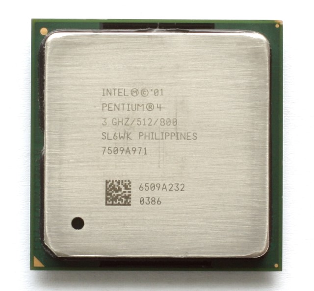
The NetBurst microarchitecture can be considered relatively unsuccessful, but processors based on it have several achievements: the Pentium 4 became the first x86 processor to reach a clock speed of 3 GHz, and the first 64-bit x86 processor from Intel. In addition, the Pentium D processor was created based on the Pentium 4, which became Intel's first dual-core processor.
Pentium M and its descendants
Almost immediately after the appearance of mobile Pentium 4, it became clear that the NetBurst architecture, due to high heat generation and power consumption, is not suitable for laptops. Therefore, in 2003, the Pentium M processor appeared, which, in fact, was an improved and modernized version of the P6 core. This processor became the basis of the extremely successful mobile Intel platforms Centrino, which included a processor, chipset and wireless adapter Intel. It was the Centrino platform that made it possible to create the first thin and light laptops. At the same time, Intel's efforts to promote wireless networks, in particular, in Ukraine, under the auspices of the company in the mid-2000s, projects were implemented to build Wi-Fi networks in Kievsky national university them. T. G. Shevchenko and the international airport "Kyiv-Borispol".
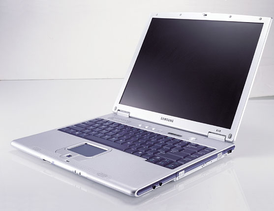
Samsung X10: one of the first thin and light laptops based on Centrino
In 2004-2005, it became clear that Pentium M processors provide more high performance than desktop processors based on the NetBurst microarchitecture. That is why the architectural solutions used in them formed the basis Core microarchitecture, which was used in both desktop and mobile processors. In 2006, the first desktop 4-core Intel processor was released - it was the Core 2 Extreme QX6700 with a clock frequency of 2.67 GHz and 8 MB of L2 cache.
From Core to Core
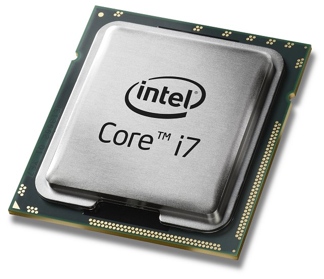
In 2008, Intel introduced the Core i7 brand, under which top processors based on the new Nehalem microarchitecture were sold. These processors received a new system bus, integrated graphics, as well as built-in memory controllers and PCIe buses. In 2009-2010, the Core i5 and Core i3 brands were also introduced, and Core 2 processors and their derivatives were pushed out of all price segments.
In 2011, processors based on the architecture entered the market Sandy Bridge, in 2012 an improved version of Sandy Bridge was introduced called Ivy Bridge, which became the first Intel processor to use the 22 nm process technology and 3D processors. In 2013 they introduced Haswell processors, and in 2014 and 2015 - Broadwell. Broadwell processors manufactured using the 14 nm process technology. These include, among other things, the Core M processor, which has a calculated heat dissipation of only 4.5 W, which allows it to be used in devices with passive cooling.
It can be noted that the growth rate of pure processor performance in Lately decreased slightly: in principle, even Core 2 processors (not to mention the first generation Core i7/i5) are sufficient for almost any task. This is due to the fact that manufacturers are paying more attention to improving the energy efficiency of processors and such a parameter as “performance per watt”. As a result, modern laptops built on energy-efficient Intel processors run on battery power for 9-12 hours and at the same time provide performance sufficient for almost any task. Just 3-4 years ago this would have been impossible.
Atom: netbooks, tablets, smartphones...
In parallel with high-performance Core processors Intel company is also developing a line of energy efficient Atom processors. They first appeared in 2008 as processors for netbooks (that is, low-end, low-cost laptops), but have since found use as chips for smartphones and tablets based on operating systems Android and Windows. In fact, Atom, today, is the only competitor to various chips based on the ARM architecture. In 2014, 46 million tablets based on Atom processors were released.
Quark: smaller than Atom
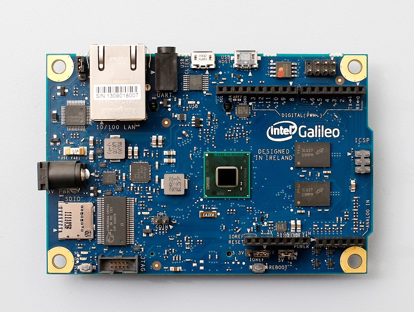
Intel Galileo: Development Board with Quark Processor
The newest family of Intel processors is the Quark line. These are very simple processors, architecturally close to the original Pentium. Each processor also includes all the controllers needed to build a complete device. These processors are intended primarily for creating embedded solutions integrated into the Internet of Things. For enthusiasts and developers, Intel releases Intel boards Galileo with Quark processors, these boards are compatible with Arduino and can be used to create your own projects and perform various automation tasks.
Today we are so accustomed to modern realities that we take them for granted. A smartphone in our pocket or a laptop in a bag seems to us not a miracle of technology, but something ordinary. But it all started with a tiny chip containing 2,300 transistors and operating at a clock frequency of 740 kHz. Sometimes it’s worth looking back to appreciate the scale of the journey you’ve made.
The Pentium D series chips were the first desktop processors to include 2 compute modules on a single silicon chip. It was this execution that allowed them to increase performance in tasks that required multiple physical cores. It is the series of these innovative central processors that will be discussed in this material.
Background of appearance
At the beginning of 2005, a very problematic situation arose in the world of processor solutions: further increasing the clock frequency was no longer possible, but it was still necessary to increase performance. Therefore, it was necessary to make certain changes to the existing organization of personal computers, the essence of which was that 2 computing modules began to be manufactured on one chip. When running single-threaded applications, performance remained at the same level. But in the case of running program code already optimized for 2 cores, this arrangement made it possible to obtain a significant increase in performance, which in some cases could reach 30-40 percent. The first such chip was the Pentium D processor. Essentially, there was no great novelty in the semiconductor crystals of this product for the reason that these were well-known Pentium 4 code processing modules. Only in the latter there was only one core, but in the Pentium D there were already two of them.
Niche of processors of this family
The first Pentium D were positioned by Intel as affordable flagship solutions with a high level of performance. Moreover, as noted earlier, the data processor devices had 2 cores on one silicon substrate. One step lower in the Intel product segment at that time was the Pentium 4 with NT support. They had one physical block and two logical ones. That is, the program code for such solutions could be processed in 2 threads. As a result, they provided an average level of performance within the LGA775 platform. The Celeron series processors were aimed at the office systems niche. Modest specifications were not allowed to be used in any other areas.
What was included in the delivery list?
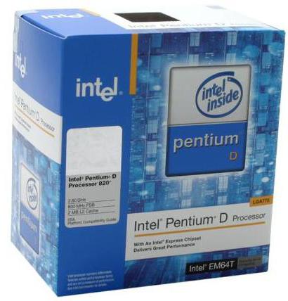
In two configuration lists one could find a Pentium D series CPU from Intel. One of them is extended and is called BOX. The manufacturing company included the following:
Branded cardboard box.
Transparent plastic case for safe transportation of the processor device.
Cooling system developed by Intel. It included an air cooler and a special modification of thermal paste, which contributed to improved heat dissipation from the CPU.
Brief instructions for use in paper form.
Sticker with the processor family logo.
Warranty card.
This delivery option was most optimally suited for using the CPU in nominal mode. If it was planned to “overclock” the processor, then the TRAIL package looked preferable. It was almost completely identical to the list of BOX supplies. The only difference was the absence of a cooling system. In this case, it had to be purchased separately. As a rule, the TRAIL configuration option was purchased by computer enthusiasts, who then equipped their PCs with an advanced cooling system. This made it possible to overclock the computer and increase its performance.
Processor socket. Architectural features
Any chip from the Pentium D line should have been installed in the LGA775 socket. Their characteristics indicated that not all motherboards on this platform supported such CPUs. Therefore, when assembling a new computer system, it is imperative to check the list of supported processor models and find “Pentium D” in it. The same procedure must be followed in the case of upgrading a personal computer. As noted earlier, 2 cores of conventional Pentium 4 crystals were part of the Pentium D. Due to this arrangement of the substrate, the temperature increased significantly during operation. To prevent overheating semiconductor base CPU, Intel was forced to significantly reduce the nominal clock speeds. As a result, performance in single-threaded tasks did not decrease significantly, but in program code, optimized for 2 threads, performance has increased.
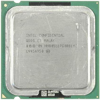
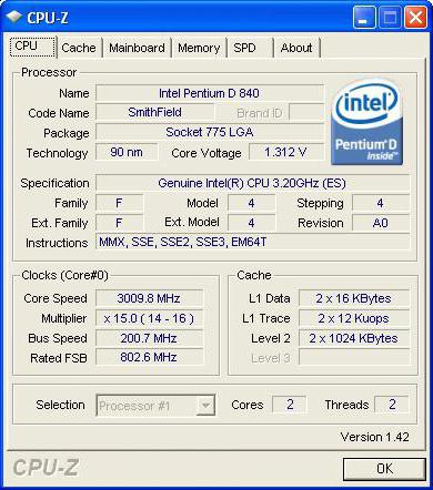
First generation Pentium D
The Intel Pentium D was first introduced in May 2005. The code name for this family is Smithfield. These CPUs were manufactured using 90 nm technology, their thermal package was stated at 130 W. The younger model with index 805 had a clock frequency of 2.66 GHz, and the data bus on the motherboard operated at 533 MHz. All other chips had a system bus frequency of 800 MHz. Moreover, both the first and second generation. The most productive CPU model was marked with the index 840. Its operating frequency was 3.2 GHz. The first level cache was 64 KB, and the second level was 2 clusters of 1 MB each. The number of transistors in this case was equal to 230 million, and the crystal area was 206 mm 2.
Second revision of this generation of chips
A year later, an updated generation of this family of chips was released. The first innovation was the technical process. Now semiconductor crystals were manufactured using 65 nm technology. This made it possible to reduce the crystal area to 140 mm 2. But at the same time, the thermal package of the CPU did not change and remained equal to 130 W. The second important update is an increase in clock speed. Its minimum value was set by the manufacturer at 2.8 GHz for chips with index 915. In this case, there were 3 flagships. Pentium D 945 and 950 operated at a frequency of 3.4 GHz, and 960 - 3.6 GHz. Another important innovation is the increase in the second level cache by 2 times - up to 2 clusters of 2 MB each. It was through the combination of these several factors that Intel was able to achieve an increase in productivity, which in percentage terms could reach 20 percent.
Price
At the start of sales, the cost of such chips ranged from $70 to $110. Taking into account the positioning and capabilities, such a price tag was completely justified. Now, quite a lot of time has passed since the start of sales, but you can still find such processors on sale. Only their prices have decreased significantly and are in the range from 30 to 50 dollars. For example, Pentium D 945 now costs 3,800 rubles. Considering that the main niche of such CPUs is office systems, such an approach to pricing is entirely justified. At the same time, the remaining components are in the same personal computer will cost much less. Therefore, Pentium D is a worthy option for assembling inexpensive PCs with low performance.
Few people know, but at the origins of the creation of the most famous in the world Intel processor There were also Soviet specialists and engineers at Pentium. At one time, the USSR achieved quite serious achievements in creating computer equipment. An example of this is the series of Soviet supercomputers "Elbrus", which were created at the Institute of Precision Mechanics and computer technology(ITMiVT) in the 1970-1990s of the last century, the same name is given to a series of microprocessors and systems created on their basis and produced today by JSC MCST (Moscow Center for SPARC Technologies).
History of the company "Elbrus MSCT" - began in 1992, when Babayan and his colleagues and with the participation of David Dietzel, who at that time worked at Sun Microsystems, organized the “Moscow Center for SPARC Technologies”. Later, with the participation of Babayan, several more companies were created: “Elbrus 2000”, “Elbrus International”, which form “Elbrus MCST”.
The company worked both on orders from foreign companies: Sun, Transmeta (it was this company that David Dietzel eventually moved to), and also carried out work on orders from the Russian government. First of all, these are the Elbrus 90-micro computer systems used in the Russian army, based on their own processors of the MCST R series. For their creation, Babayan and his colleagues at one time received state awards.
However, the history of “Elbrus” itself much longer. The first computer with this name was created back in 1978 at ITMiVT im. S.A. Lebedev Academy of Sciences of the USSR under the leadership of B.S. Burtsev and with the participation of Boris Babayan, who was one of the deputy chief designers. The main customers of Elbrus computers were, of course, the military.
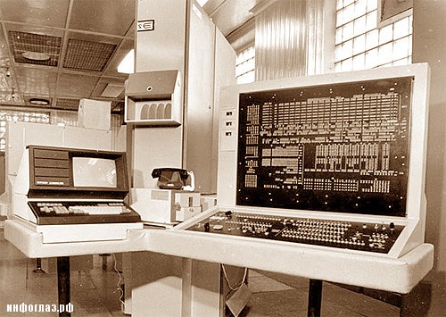
The first Elbrus computer had a modular architecture and could include from 1 to 10 processors based on medium integration circuits. The speed of this machine reached 15 million operations per second. The amount of RAM, which was common to all 10 processors, was up to 2 to the 20th power of machine words or, if we use the now accepted notation, 64 MB. However, the most interesting thing about Elbrus-1 was its architecture. The supercomputer created in the USSR became the world's first commercial computer to use superscalar architecture. Its mass use abroad began only in the 90s of the last century with the advent of affordable Intel Pentium processors on the market.
As it turned out later, similar developments existed before “Elbrus” at the IBM Corporation, but these works were closed and did not lead to the creation of a commercial product. True, in a number of publications information appeared that when designing “Elbrus”, the developments of foreign companies were used as the basis. However, those involved in the creation of the Soviet supercomputer do not agree with this position. In one of the interviews with V.S. Burtsev, the chief designer of Elbrus, noted that when creating the computer, the designers tried to use the best practices of both domestic and foreign developers. And the architecture of the Elbrus was influenced not only by Burroughs computers, but also by the developments of companies such as Hewlett-Packard, as well as the experience of the creators of BESM-6.
At the same time, a considerable part of the developments was original, including the superscalar architecture. In addition, special input/output processors could be used to organize the transfer of data streams between peripheral devices and RAM in the computer. There could be up to 4 such processors in the system; they worked in parallel with the central processor and had their own memory.
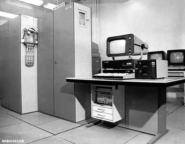
The next stage of work was the creation of the Elbrus-2 computer. These computers went into mass production in 1985. In its own way interior architecture they were not very different from Elbrus-1, but they used a new element base, which made it possible to increase the maximum performance to 125 million operations per second. The computer's RAM capacity has increased to 16 million 72-bit words or 144 MB. Maximum throughput I/O channels of Elbrus-2 was 120 MB/s.
These computers were actively used in the USSR in areas that required a large number of calculations, primarily in the defense industry. The Elbrus-2 computers were operated in nuclear research centers in Chelyabinsk-70 and in Arzamas-16 at the MCC; finally, this particular complex, starting in 1991, was used in the A-135 missile defense system, as well as at other military facilities in the country.
In addition to the two computers listed above, the Elbrus 1-KB general purpose computer was also produced, the creation of this computer was completed in 1988. Until 1992, 60 such computers were produced. They were based on Elbrus-2 technologies and were used to replace outdated BESM-6 machines. At the same time, there was full backward software compatibility between Elbrus 1-KB and BESM-6, which was supplemented by new operating modes with increased bit depth of numbers and addresses.
The creation of the Elbrus computers was appreciated by the leadership of the Soviet Union. For the development of Elbrus-1, many engineers were awarded orders and medals. Boris Babayan was awarded the Order of the October Revolution, his colleague V.V. Bardizh - Order of Lenin. For the development of Elbrus-2, Babayan and a number of his colleagues were awarded the Lenin Prize, and general designer V.S. Burtsev and a number of other specialists - State Prize.
After completing work on the Elbrus-2 computer, ITMiVT began developing a computer based on a fundamentally new processor architecture. The project, which was named quite simply - “Elbrus-3”, was also significantly ahead of similar developments in the West. Elbrus-3 was the first to implement an approach that Boris Babayan calls “post-superscalar”. Intel Itanium processors, as well as Transmeta chips, had exactly this architecture in the future. It is worth noting that in the USSR, work on this technology began in 1986, and Intel, Transmeta and HP began implementing work in this direction only in the mid-1990s.
Unfortunately, Elbrus-3 was never put into mass production. Its only working copy was built in 1994, but at that time no one needed it. A logical continuation of work on this computer was the appearance of the Elbrus-2000 processor, also known as E2K.
According to Boris Artashesovich Babayan, the chief architect of the Elbrus line of supercomputers, superscalar architecture was invented in Russia: “- In 1978, we made the first superscalar machine, Elbrus-1. Now in the West they make only superscalars of this architecture. The first superscalar appeared in the West in 1992, ours in 1978. Moreover, the version of the superscalar that we made is similar to the Pentium Pro that Intel made in 1995«-.
Elbrus also confirms its historical primacy in America. In the same Microprocessor Report article, Keith Diefendorff, developer of the Motorola 88110, one of the first Western superscalar processors, writes: "- In 1978, almost 15 years earlier than the first Western superscalar processors appeared, the Elbrus-1 used a processor that issued two instructions per clock cycle, changed the order of execution of instructions, renamed registers and executed by assumption«-.
In 1991, Mr. Peter Rosenbladt from Hewlett-Packard visited Elbrus (then still ITMiVT) and received comprehensive documentation on Elbrus-3. It later turned out that it was then that HP began a project that led to the joint development of the Merced EPIC processor with Intel. Its architecture is very similar to Elbrus-3, and the differences are mainly due to simplifications made in the Intel microprocessor.
According to B.A. Babayan, Peter Rosenbladt proposed cooperation with HP. But Babayan chose Sun (the first meeting with Sun management took place back in 1989). And in 1991, a contract was signed with Sun. Sun officials know that Elbrus took part in the development of the UltraSPARC microprocessor, optimizing compilers, operating systems (including Solaris), Java tools, and multimedia libraries.
The E2k project was originally funded by Sun. Now the project is completely independent, all intellectual property on it belongs to Elbrus and is protected by approximately 70 US patents. B.A. Babayan explains “- If we had continued to work with Sun in this area, everything would have been owned by Sun. Although 90% of the work was done before Sun appeared«-.
At Sun from 1992 to 1995, Elbrus worked with renowned microprocessor architect Dave Dietzel. As B.A. says Babayan, "- Then Dave formed his own company, Transmeta, and began working on a car very similar to ours. We continue to maintain close contact with Ditzel. And he really wants to cooperate with us"-. Little is known about Transmeta's future product. It is known to be a VLIW/EPIC microprocessor with low power consumption, binary compatibility with x86 is ensured by dynamic translation of object code.
E2K vs Itanium
The 64-bit Intel Itanium processor did not live up to expectations and on paper was much inferior to Elbrus-2000.
From 1994 to 1998, nothing was heard about the work of Boris Babayan’s team - the Russians were preparing a sensation. In 1998, without much fanfare, Babayan and Co. (about 400 employees) renamed themselves the Elbrus company.
Meanwhile, foreign competitors did not sleep. In 1989, Intel and Hewlett-Packard joined forces to create a new generation processor - Itanium (code name - Merced). Itanium was supposed to incorporate all the latest developments and become the crown of processor technology. Many expected the new processor to dominate the server, workstation and perhaps desktop market, displacing all others. Merced's design frequency was 800 MHz, its heat dissipation level was 60 W, and its L3 cache was 2 to 4 MB. At the same time, the processor had to become 64-bit.
The completely real R500 processor from MCST was a faded echo of the promising Elbrus-2000.
Day X came on February 25, 1999, when at the Microprocessor Forum conference Boris Babayan personally rose to the podium and loudly declared that his company had developed the Elbrus-2000 (E2K) microprocessor, which was far ahead of the vaunted Merced in all characteristics. The entire computer community froze in anticipation. Instead of the planned two hours, Babayan spoke for four hours. Answers were given to questions regarding competition from Western companies and the prospects for entering the market of a microprocessor and computers based on it. At some point, Boris Babayan shocked the public by declaring that $60 million was needed to produce a trial batch of Elbrus-2000 processors. This figure scared off all potential investors. Of course, all of Babayan’s promises were pure theory - no engineering samples or prototypes were shown.
Computer world legend Gordon Bell, who, while working at DEC, created PDP and VAX line computers and now heads the Microsoft research division (Telepresence Research Group), popularizes the Elbrus E2k project at international conferences.
His lecture entitled “The Next Ten Years in Supercomputing” opened the International Symposium on High Performance Computing in Japan on May 26, 1999, and the fourteenth Mannheim Conference on Supercomputing on June 10. Mannheim Supercomputer Conference) in Germany. Both times, Dr. Bell devoted part of his lecture to talking about E2k. In a slide called “Russian Elbrus E2K”, he provides a table where he evaluates E2k and Merced. Moreover, the comparison is clearly not in favor of Intel's brainchild.
Below is a table from Gordon Bell's report.
| Microprocessor | E2K | Merced |
|---|---|---|
| Clock frequency, GHz | 1.2 | 0.8 |
| Performance, SPECint95 / SPECfp95 | 135 / 350 | 45 / 70 |
| Crystal size, mm2 | 126 | 300 |
| Energy consumption, Watt | 35 | 60 |
| Bus bandwidth, GB/sec | 15 | n/a |
| Caches (KB) | 64 / 256 | n/a |
| Peak performance, GFLOPS | 10.2 | n/a |
| Planned delivery start time | 4th quarter 2001 | n/a |