- Ryzen Threadripper 1950X 3.4Ghz 16core 40Mb 14nm"> Ryzen Threadripper 1950X 3.4Ghz 16core 40Mb 14nm
- Ryzen Threadripper 1920X 3.5Ghz 12core 38Mb 14nm"> Ryzen Threadripper 1920X 3.5Ghz 12core 38Mb 14nm
- Inexpensive tablet characteristics should be
You can mark sections of text that interest you,
which will be available through a unique link in the address bar of the browser.
Support for virtualization software for safer, more efficient execution and improved results in virtualized systems. Designed to make better use of performance by automatically and on-the-fly adjusting performance levels and features that result from corresponding processor performance requirements.
All of this has meant new sockets and new motherboards, which may cause some confusion between future buyers who want to build a computer or want to upgrade their hardware. In the following table we see the sockets, chipsets and family of compatible processors.
Introduction to Socket FM2. Review and testing of Gigabyte F2A85X-UP4 on AMD A85X chipset
I.N. 03.10.2012 00:00 Page: 1 of 7| | print version | | archive
- Page 1: Introduction, Socket FM2: processor cooling system, new A85X chipset, review of the Gigabyte F2A85X-UP4 motherboard: packaging and bundle
- Page 2: Gigabyte F2A85X-UP4: board design and features, cooling system
- Page 3: Gigabyte F2A85X-UP4: design and features, CO (continued), specifications
- Page 4: BIOS Setup Features
- Page 5: BIOS Setup Features (continued)
- Page 6: Test bench, start-up, checking the accuracy of the set voltages and the operation of Load-Line Calibration, checking overclocking
- Page 7: Overclocking test, Trinity integrated video core, conclusion
Introduction
So, the official release of the new AMD platforms in the design of Socket FM2. Of course, the processors themselves are quite interesting, but what is the CPU? A piece of silicon on a substrate, closed with a metal lid, at the price of a certain number of banknotes. Nothing more. This is just one element of the system called "computer". But the skeleton that binds and carries almost everything is the motherboard. It is on it that the functionality that the final system will receive, as well as how fully the potential of the processor will be realized, largely depends.
Final thoughts and recommendations
When connecting your latest purchase to one of these motherboards, keep the following tips in mind. Hope this guide was helpful and don't forget to read our guide. Which platform do you like the most? 
Thanks to this architecture, it became possible to start developing 64-bit operating systems. 
Cache memory is small, very fast, and maintains important data from processes running on the processor. 
This is a computer part that contains a series of instructions that allow you to perform calculations and operations. Dual-core: The term is used to refer to any dual-core processors. 
The technology is activated when the processor notes that the processing power is insufficient to perform some tasks. 
This practice is very common among enthusiasts who want to get better performance or just break records. Platform: A term used to represent a set of technologies that forms a new processing standard. When used in accordance with product specifications.
- The first chips in this series had approximately 275,000 transistors.
- It was abandoned with the arrival of a bulldozer.
- This feature increases the frequency of some cores and disables others.
- Architecture: A set of designs and specifications behind the hardware.
- The contacts in this socket are in a spherical format.
- This will bring new extensions and the models will be compatible with the socket series.
- Still in production, the line is calculated on two cores.
- The acronym is used as a synonym for processor.
- Now extinct, the Durons have been replaced by the current Semprin.
- There are currently three generations of this line.
- As the name suggests, it contains 155 contacts.
- All models are manufactured with 32nm nanotechnology.
- Lithography: part of the processor fabrication process.
- A commonly used term for a report on the construction of nanotechnology.
- The module is a set of two cores.
- Processors in this series can have up to six cores.
- Models of this line have only one core.
- It has models equipped with one and two cores.
- It is the integration of multiple computer components into a single circuit.
- Adaptive refresh rates vary by monitor.
- Check with your monitor manufacturer for specific features.
- Not all technologies are compatible with all system configurations.
- Check with your system manufacturer about the specific features of your model.
Socket FM2
Processor cooling system
new platform, new processor- it's always interesting. Well, almost always. However, in addition to interest in performance and price, there is a question of compatibility, for example, with old cooling systems.

With the new Socket FM2 socket, AMD did not change its traditions - the fastening of the CPU cooling system remained unchanged and is either two separate plastic elements (which appeared on Socket AM3+), or a single plastic frame (more early version). On the reverse side, the motherboard is protected from deflection by a plate - plastic with similar latches or metal with bolts (at the choice of the manufacturer). The location of the holes has not changed. For comparison, here is a photo of Socket FM2 and Socket AM3 mounts (mother Gigabyte board GA-MA790XT-UD4P).
After all, some of them may marry better with what you're going with your computer and your pocket. To better target your search, we categorize the units into used profiles: internals, interested in games, and finally enthusiasts. So before you read a bit about the options in this text, consider that there are a few intermediate models among those listed here.
Of course, there is no separate fee for performance, but this is a good value option and is great for a user who wants to set up a computer for Internet access, play more simple names, such as browser games and watching videos in the end.

The mount has remained virtually unchanged since the days of Socket 754, which, by the way, celebrated its ninth anniversary last month. Thus, any cooling system compatible with Socket 754/939/AM2/AM2+/AM3/AM3+/FM1 will do:
 Thermaltake Big Typhoon 120 VX
(2007) from the author's vaults
on a Socket FM2 motherboard.
Ignore: For everyday activities and even gaming, the processor is absolutely capable of running any current game- provided that it is well accompanied by memory and a video card. It is still hard to find in Brazil due to the recent launch. Then you will find out which platforms are currently used by the two brands, considering the offer of processors in the Brazilian market.
The socket name can be parsed. An interesting aspect of the platform is the design to prevent the use of unsupported processors in the socket, which can cause permanent damage. There is also a locking mechanism that provides correct installation correct processor.
Enviable constancy.
New A85X logic set
Before getting to know motherboard, it is necessary to at least briefly consider its basis - the chipset. After all, in many ways, the possibilities of the board depend on the set system logic on which it is based. One important thing to note here Socket difference FM1/FM2 from Socket AM3/AM3+: all FM1/FM2 chipsets are single-chip chipsets, actually consisting of a southbridge, since almost the only element north bridge- the main PCI-E controller, used primarily for graphics slots, is now part of the processor. Why "main"? Yes, because the second PCI-E controller, modest in terms of characteristics (only a few lines), used for peripherals, has not disappeared from the south bridge.
In this tutorial, we will list all types of sockets already released to date, with a list of compatible processors. At first processor socket was compatible with only one type of processor. Using the same pinning pattern for multiple processors allowed the user or technician to set different models processors on the same motherboard by simply removing old cpu and placing a new processor. Of course, for this, the motherboard had to be compatible with these processors and correctly configured.
Together with the processors codenamed Trinity, AMD also introduced a new chipset A85X (codename "Hudson D4"), which is the development of the previous generation of AMD chipsets - A55 and A75, without carrying anything revolutionary for the "Comal" Socket FM2 platform, which seen from its characteristics. As a comparison, I will give the characteristics of AMD's leading chipset for Socket AM3+, or rather, its south bridge SB950.
Even though it doesn't have an official name, let's call it a socket. So socket 2 accepts the same processors as socket 1 and more, and so on. As you can see, the socket and pin layout of these early processors was a bit confusing, as the same processor could be installed in multiple socket types.
For the following processors, manufacturers have used a simpler scheme, where each processor can only be installed on one type of socket. Runs on 32-bit: not specified. Runs on 64-bit virtualization: not specified. Monitor capacity: Not specified.
| A85X | A75 | A55 | SB950 | |
| Process technology, nm | 65 | 65 | 65 | 65 |
| Thermal pack, watt | 7.8 | 7.8 | 7.6 | 6.0 |
| Processor communication bus | Unified Media Interface 2.0 (UMI 2.0) 2GB/s | Unified Media Interface 2.0 (UMI 2.0) 2GB/s | Alink Express III (2GB/s) | |
| Support for graphics tandems | AMD CrossFireX AMD Dual Graphics | AMD CrossFireX AMD Dual Graphics | AMD CrossFireX AMD Dual Graphics | AMD CrossFireX NVIDIA SLI |
| Disk subsystem | 8 SerialATA III 6Gbps ports Support for RAID 0, 1, 5, 0+1 and JBOD, AHCI, NCQ, eSATA and port splitters (including FIS-based) | 6 SerialATA III 6Gbps ports Support for RAID 0, 1, 0+1 and JBOD, AHCI, NCQ, eSATA and port splitters (including FIS-based) | 6 SerialATA II 3Gbps ports Support for RAID 0, 1, 0+1 and JBOD, AHCI, NCQ, eSATA | 6 SerialATA III 6Gbps ports Support for RAID 0, 1, 5, 0+1 and JBOD, AHCI, NCQ, eSATA and port splitters |
| Built-in memory card controller | Secure Digital 2.0 (SDHC) up to 32 GB inclusive | absent | absent | |
| USB 1.1 support | 2 ports (one UHCI host controller) | 2 ports (one UHCI host controller) | 2 ports (one UHCI host controller) | 2 ports (one UHCI host controller) |
| USB 2.0/1.1 support | 10 ports | 10 ports (three separate EHCI host controllers) | 14 ports (three separate EHCI host controllers) | 14 ports (three separate EHCI host controllers) |
| USB 3.0/2.0 support | 4 USB port 3.0 (one xHCI host controller) | 4 USB 3.0 ports (one xHCI host controller) | absent | absent |
| PCI-E for communication with peripherals/controllers | 4 lanes PCI-E 2.0 + | 4 lanes PCI-E 2.0 + 4 lanes PCI-E 2.0 by CPU | 4 lanes PCI-E 2.0 + 4 lanes PCI-E 2.0 by CPU | 4 lanes PCI-E 2.0 + 6 lanes PCI-E 2.0 by northbridge |
| PCI | 3 slots (can be used for additional controllers) | 3 slots (can be used for additional controllers) | 4 slots (can be used for additional controllers) |
As mentioned above, the whole difference between chipsets for AM3/AM3+ and FM1/FM2 lies in the fact that in the latter the northbridge of the logic set "moved" to the processor, so the similarity between them becomes even greater than it at first glance follows from the above tables.
If in the case of Socket AM3 (+) Hyper Transport 3.1 (6.4 GT/s) is indicated - the connection between the processor and the north bridge, then in the case of FM1 / FM2, the name of the communication bus between the bridges is actually given (after all, the north bridge itself is now in the processor) - Unified media interface. And for Socket AM3/AM3+, the connection between bridges is called Alink Express. Only the essence is the same: in both cases, these are four lanes of PCI-E version 2.0. Doesn't look like anything? If you look closely, you get a very persistent feeling that, under the guise of A**, users actually got a converted and slightly modified traditional south bridge of AMD chipsets. Which, however, is not too surprising, given the realities of today.
New A85X logic set
Experience breathtaking sound. Try a new level of immersion. Many popular, modern software titles may require quad-core processors to run properly. Share your experience with your personal preferences, whether performance, efficiency or low level noise. 4.
More than just increasing clock frequency
Now bundled with a selection of powerful, near-silent coolers, you can choose the perfect solution for your entire system. 4.
New, quiet and powerful coolers
Expanded learning opportunities. Helps software virtualization work more reliably and efficiently, providing a better experience with virtual systems.Something removed, something, on the contrary, added to maintain both technical and marketing levels. For example, the built-in SDHC card controller is not at all superfluous for mobile PCs, where, among other things, FM1 / FM are positioned, and in desktop computer it will not interfere at all (if the case manufacturer takes care of implementing such functionality). But a special abundance of PCI and PCI-E ports is unlikely to be needed, so their number was reduced, which certainly made it possible to both simplify the crystal and save a little in power consumption. In fairness, it is worth noting that despite the functionality of the A55, which is more modest than that of the SB950, the TDP of the first is for some reason noticeably higher.
Designed to provide more efficient performance by automatically and instantly adjusting performance states and characteristics based on processor performance requirements. The base of Military Grade 4 is based on core elements that increase your stability even in the worst conditions. Moisture and heat protection ensure your system can withstand any environment.
Various processor models

This allows you to precisely control your components. ![]()
Low throughput, recommended processors. This solution allowed much higher locking forces through the load plate with the locking lever, providing more stability and better heat transfer - better cooling.
There is also another noteworthy point in the configuration of PCI-E lanes: the competing Intel platforms- LGA 1155 - there are similarly two PCI-E controllers, they are also located in the processor and chipset, the number of lines is the same - 16 + 8. But the Intel CPU supports only sixteen lines used only for graphics system, and the chipset itself provides eight more lines (which, by the way, are often enough for manufacturers to implement all the functionality “with a scratch”, and as a result, both switches and switches are used). The communication bus between the processor and the chipset is called the Direct Media Interface (DMI) and, funny, physically it's still the same PCI-E x4 as AMD has. with the same throughput.
Turning off the stop on the left raises the load plate so the processor can be placed over the pins. Supports multiple processor configurations. In general, it was better to buy a suitable processor for this type of socket. Future versions supported quad-core processors, for a total of eight cells per system.
Test stand configuration
A clear trend for those who follow the world of chip design is that work pressure should be kept low. The benefits of reduced voltage are various. The clearest thing is that at lower voltage we usually have lower consumption. By consuming less power, you spend less to run the system, something more important in laptops that rely on battery. The emphasis on autonomy has led manufacturers to make significant progress in lowering the power supply, since it greatly affects the battery.
As a result, one can see a great similarity between the two platforms. Except for two "buts". The first is that Intel has support for PCI-E 3.0 (processor controller Ivy Bridge, the chipset itself, even the new Z77, still offers 2.0), and AMD refused 3.0, saying that it doesn’t hurt, it’s needed (at the same time, modern AMD video cards fully support this same PCI-E 3.0). Therefore, Socket FM2, despite its novelty, is exclusively PCI-E 2.0. Secondly, both platforms offer eight PCI-E lanes for peripherals in the form of expansion cards and additional controllers on the board. But for AMD, half of the lines are connected directly to the processor, while for Intel, all eight lines from the south bridge (together with four SATA2, two SATA3, four USB 3.0, fourteen USB 2.0, etc.) are tied to exactly the same bandwidth bus.
The second big advantage is that with less tension and therefore less consumption, there is less heat. Processors that are cooler can be put into smaller systems and last longer. The third advantage is that a new processor that consumes less can be made to run more fast work. Reducing voltage is one of the key factors in achieving higher frequencies. Therefore, the lower the voltage, the less time it takes for the signal to change from low to high.
Most likely, it is precisely because of this that Intel has such a variety of SATA versions, and as a result, users need to understand the colors of SATA ports, which is the second version, and which is the third (by the way, the question is not as easy as it might seem - sometimes color designation back all the way to the opposite) to connect a freshly purchased SSD. AMD, as a rule, does not force users of its products to think about such technical nuances.
Well, as in the case of AM2/AM3/AM3+, the set of logic for Socket FM2 is not a constant. The former can have both 790FX and SB600 together, as well as 790X paired with SB850. For FM2 both A85X, A75 and A55 can be used. They are applied: A75 and A55 will not leave the market, just now the platform with AMD APUs will be divided into three segments - lower (A55), middle (A75) and older (A85X). Accordingly, almost all manufacturers have prepared (or are preparing for this moment) products on all chipsets. So, Gigabyte introduced four models:
- Gigabyte GA-F2A55M-DS2 based on A55 for the budget segment;
- Gigabyte GA-F2A75-D3H and GA-F2A75M-D3H based on A75 for the middle segment;
- Gigabyte GA-F2A85X-UP4 on A85X for the older segment.
Seemingly complex names are actually easy to decipher and characterize their carriers:
- GA - Gigabyte;
- F2 - Socket FM2;
- A** - chipset used in the basis of the board;
- The letter "M" denotes the mATX format, "X" - support for NVIDIA SLI technology (although in this case there is no explicit mention of its support, so, most likely, here "X" is only part of the chipset name and, perhaps, is left for " beauty");
- DS2, D3H, UP4 - briefly describe the features and class of the product, for example, "P" indicates that the board belongs to the UltraDurable 5 product family.
In the near future, the release of two more motherboards with the HD2 index at the end is expected. These will be mid-range products. Well, the subject of this review will be the Gigabyte top-class model for Socket FM2 - motherboard GA-F2A85X-UP4 based on AMD A85X chipset.
Overview of the Gigabyte F2A85X-UP4 motherboard based on the AMD A85X chipset
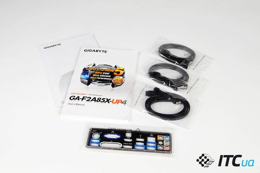
Packaging and equipment
Despite the new AMD platform, Gigabyte did not make any changes to the box design.
Both front and back side packaging is replete with references to various technologies, including branded ones, that have found application in this product

Let's consider them in a little more detail.
- Most of the space is allocated for the description of the processor power supply system based on DrMos chips (at the same time, the word "DrMos" itself is not mentioned for obvious reasons - it has been used by another motherboard manufacturer for a long time). Moreover, it is directly indicated that high-performance IR3550 microcircuits are used and their advantages are described.
- GIGABYTE Digital Power Engine provides two separate power converters for the processor itself and the integrated GPU.
- The use of copper layers with double the thickness.
- 3D BIOS / DUAL UEFI BIOS - the motherboard uses UEFI BIOS, which has two versions of the interface - familiar and pseudo-3D (3D). DUAL means the presence of two chips: the main one and the backup in case the contents of the first one are damaged.
- DirectX 11 indicates full support for the integrated graphics core of AMD APUs.
- 333 Onboard Acceleration implies that the motherboard has USB 3.0 ports with three times the current and SATA 6 Gb / s ports.
- Using only Japanese polymer capacitors.
- GIGABYTE On/Off Charge is Apple USB accelerated charging technology.
- Support for Lucid Universal MVP technology, which allows you to quickly switch between the integrated graphics core of an AMD APU and a discrete graphics card, as well as combine their graphics power.
- Support for AMD Eyefinity, AMD Dual Graphics and AMD CrossFire technologies.
- Triple-Monitor support means the ability to run three monitors simultaneously (AMD Eyefinity).
- dual-link DVI port implies the presence of a Dual link DVI-D port on the rear panel of the motherboard, capable of outputting an image with a resolution of 2560 by 1600 pixels, which is important when using monitors with a large diagonal.
- DVI and HDMI ports available.
The interior of the box is quite standard for a middle-class product: no transparent windows, nested boxes (one or more) and so on.
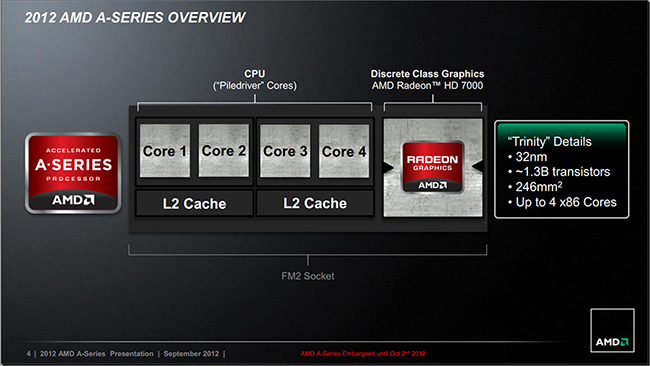
Company AMD introduced the second generation of desktop APUs. chips Trinity are based on the improved Piledriver architecture and also have a powerful integrated video core. Mobile versions new generation processors from AMD have been offered as part of laptops for almost half a year. An attractive combination of consumer parameters allowed the company to increase its share in this segment. Let's see if the desktop versions of Trinity, designed for the new platform, will be so successful Socket FM2.
APU Trinity
What are the new hybrid processors codenamed Trinity? In the maximum configuration, these chips include a quad-core x86 computing unit with the most advanced AMD architecture at the moment - Piledriver. This further development Bulldozer architecture, which is used for the fastest AMD FX series chips. In addition, a graphics core is placed on the chip, which the manufacturer refers to the Radeon HD 7000 series.
Trinity, although they are the successors of the Llano processors, however, there is practically nothing left in common between them. Both the computing part and the graphics part in this case are not just improved, they are fundamentally different. Perhaps the only thing that connects the APU of both generations is the 32-nanometer process technology, which is also used for Trinity. Of course, a more advanced technical process would be preferable here, but the production facilities of GlobalFoundries are not yet ready for the mass production of chips using technology thinner than 32 nm.
Trinity's die area is 246 mm² and contains 1.3 billion transistors, while the Llano chip's silicon wafer is 228 mm² and carries 1.18 billion transistors (after a recent update by the manufacturer). The packing density remained about the same, the area increased by about 8%, while the number of semiconductors increased by 10%. Given the timing of the development of the 32-nanometer process technology, we assume that the cost of production of crystals, if increased, then only slightly.

What's new in Trinity? The dual-channel DDR3 memory controller officially supports operation in modes up to DDR3-1866, while it also became possible to use modules with a reduced supply voltage (1.25 V). As you can see, almost half of the crystal is occupied by the graphic part. The integrated GPU has an architecture inherent in chips for discrete adapters of the family Northern Islands. An important innovation is the AMD HD Media Accelerator video encoding/decoding unit. The northbridge functions of the chipset are, of course, now integrated into the processor. In terms of computing power, Trinity has a couple of dual-core x86 modules. Within each of them, the cores are partially dependent, as they use some common resources, in particular, instruction prefetch and processing blocks. real numbers(FP). Each module has a dedicated 2 MB L2 cache segment. L3 cache memory is not provided here - this is the prerogative of the AMD FX series CPUs. For communication with external devices, the processor has at its disposal 24 PCI Express lanes. Note the support for HDMI, DisplayPort 1.2 and DVI interfaces.
Trinity processors initially operate at fairly high clock speeds. If Llano chips have just approached the 3 GHz bar, then the older model from the new APU family normally operates at 3.8 GHz, with the ability to accelerate up to 4.2 GHz. Trinity received the latest modification of the dynamic auto-acceleration mechanism AMD Turbo Core 3.0, which, depending on the nature of the load, can automatically increase the frequency of the CPU. Each processor model has its own range: from 200 to 600 MHz.
Integrated graphics
Introducing the term APU(Accelerated Processing Unit), the company initially wanted to emphasize the importance of the integrated graphics unit. Integrated graphics core Trinity, dubbed Devastator, uses architecture VLIW4, which was used for the Radeon HD 6900 of the Northern Islands family. Obviously, the developers have not yet managed to optimize for the needs of the APU new architecture GCN (Graphics Core Next), which is used in the GPU for discrete video cards of the Radeon HD 7000 series.
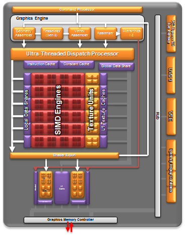
Recall that the graphics part of the Llano chips has the VLIW5 architecture. The computational units it includes can theoretically perform more operations in parallel than those with VLIW4. However, in real tasks the latter are more efficient. In addition, VLIW4 stream processors, all other things being equal, can operate at a higher clock frequency. It is quite difficult to draw parallels here, but some quantitative indicators are curious. IN full version the Llano graphics core contains 400 computing units, while the Trinity GPU has 384, but in the latter case, the nominal operating frequency of the graphics unit is 800 MHz, while the predecessor has 600 MHz.
The Devastator core includes 24 texture units and 8 rasterizers. AMD emphasizes that in this case the tessellation processing unit is noticeably accelerated. A hardware block is allocated for working with video data AMD HD Media Accelerator, which includes the most advanced UVD3 video decoding module inherited from the Radeon HD 6000/7000 processor. In addition, the processor contains the AMD Accelerated Video Converter video transcoding unit. Functionally, it is similar to Quick Sync, which Intel uses in its processors.
In general, the Trinity graphics core has excellent functionality. It boasts full support for DirectX 11 with Shader Model 5.0, OpenCL 1.1 and DirectCompute 11. At the same time, the new APUs allow you to connect up to four independent display devices, moreover, support for Eyefinity technology is also announced. Also noteworthy is the support AMD Steady Video 2.0, which allows you to improve the quality of your video by helping to eliminate the effect of shaky images during handheld shooting.
Like its predecessors, Trinity processors have the ability to operate in Dual Graphics, combining the efforts of an integrated GPU with a discrete graphics card. However, in this case, we are still talking about devices entry level from the Radeon HD 6500/6600 lines.
The manufacturer recommends using the Radeon HD 6670 to help the A10 chips, the Radeon HD 6570 is offered for the A8 and A6, while the HD 6450 is offered for the A4. a potential owner of a Socket FM2 system already has a video card that can be used as an additional accelerator. The intentional purchase of an adapter of the required class for use in Dual Graphics mode, although it has the right to exist as a deferred upgrade option, however, in general, it loses to the idea of acquiring a faster graphics adapter, which will cost a little more, but in games it will be noticeably more productive than the proposed bundle.
Piledriver architecture
The Piledriver architecture is an upgraded version of the Bulldozer used for the Zambezi (AM3+) chips.
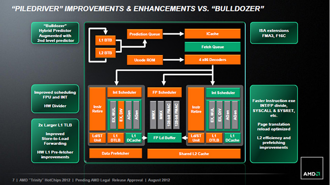
Branch prediction blocks, data prefetching have been improved, the efficiency of working with the second-level cache has been increased, the L1 TLB size has been increased, and the work of the INT and FP module load scheduler has also been improved. In addition, the new F16C instruction sets are now supported, as well as FMA3, which Intel plans to add to its Haswell chips. AVX kits are now available for new APUs, which were not supported by Llano chips. In general, Piledriver does not fundamentally differ from the Bulldozer architecture, it is a modified version with a number of improvements and cosmetic optimizations.
APU Trinity range
At the time of the launch of the new platform, the line of chips Trinity includes six models. Two quad-core processors A10 and A8, and one each A6 and A4. As you can see, the number of x86 blocks is not reflected in the name of the APU series. At the same time, there is a dependence of the chip belonging to one or another line, which is determined by the number of computing cores of integrated graphics: A10 - 384, A8 - 256, A6 - 192, A4 - 128. This is another clear example of how the manufacturer wants emphasize the importance of the graphic component.
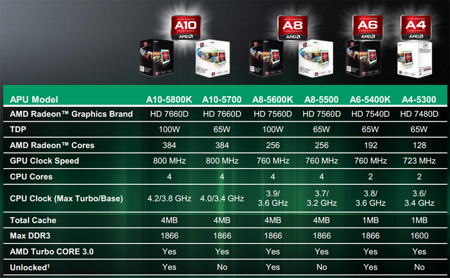
Line flagship - A10–5800K– operates at 3.8 / 4.2 GHz, its integrated GPU contains 384 computers and operates at 800 MHz. The L2 cache is 4MB and the claimed power consumption is 100W. The second "ten" has the same characteristics, except for the frequency formula. For A10-5700 the base ones are 3.4 GHz, and the dynamic auto-overclocking limit is 4 GHz. This was enough to bring the TDP down to 65W. In A8 models, in addition to a reduced number of video core processing units from 384 to 256, its operating frequency is also reduced to 760 MHz. Formulas for x86 blocks: A8-5600K– 3.6/3.9 GHz, A8-5500– 3.6/3.8 GHz. Single-module A6 and A4 chips, in addition to losing two x86 blocks, have a common L2 cache of only 1 MB. Quantity GPUs reduced to 196 in case of A6-5400K, and up to 128 - at A4-5300.
As for the cost of the new APUs, the Trinity chips actually play in the same price segment as their predecessors - $50-130. At the same time, the pricing system is interesting. Both A10s are priced at $122. Both the model with an unlocked multiplier and the chip with a lower clock speed and a blocked KU have one recommended cost, which nevertheless has a TDP of 65 W, instead of 100 W for the flagship. The situation is exactly the same with the A8 line of APUs - both models are offered at the same price of $101. For someone has more value high performance, someone prefers more economical options. And for those and for others, suitable processors will cost the same price.
As is the case with Llano processors, as well as devices from a competitor, models with the “K” index have an unlocked multiplier. Curiously, now the most affordable model with this feature costs only $67, while the price of the previous generation APU with a free multiplier started at $80. However, the A6-3670K is a quad-core model, while the A6-5400K only has one module with a couple of dependent modules.
For Socket FM2, processors with a disabled graphics core will also be available, which will complete the line of Athlon chips. Given the general concept of APU, it is obvious that separate crystals will not be produced for such models (although, given the area occupied by the GPU, this would make sense), for such processors chips will be used first of all, with certain problems in the graphic part, and if there are fewer of them than the market requires, then full-fledged crystals with a deactivated GPU will also be used.
Socket FM1 and Socket FM2 compatibility
Unfortunately for the owners of systems with hybrid chips of the first wave, the new APUs are neither forward nor backward compatible with the Socket FM1 platform. The processor socket, and, accordingly, the pins on the chip visually have a minimal difference (905 vs. 904), but a different arrangement of the "keys" does not even allow installing Trinity in the old socket.
 (left - APU Trinity, right - APU Llano)
AMD for quite a long time gave evasive answers to questions about the compatibility of FM2 and FM1 sockets, so as not to indirectly reduce the demand for processors for the latter. Now this is not necessary. Given that the new APUs are fundamentally different from their predecessors at the level of architectures, it is not surprising that they have their own power subsystem features that were not taken into account in Socket FM1. It was this fact that forced AMD to change the platform.
Chipsets
Despite the fact that Socket FM1 and Socket FM2 are incompatible with each other, the chipsets used on the previous generation platforms are quite suitable for the new one. chips AMD A55, and AMD A75 we will see in the composition of motherboards for Socket FM2. In general, there is nothing to be surprised here. Given the fact that key features chipsets are taken over by central processors, their role in modern platforms is largely reduced to servicing peripherals. And here innovation does not happen so often. If there are already certain complaints about the functionality of the AMD A55 (lack of SATA 6 Gb / s), then the AMD A75 cannot be called obsolete. The latter became the first chipset in the industry with an integrated native USB 3.0 controller. And the rest of the "kit" is quite on the level.

To make the announcement of Socket FM2 even brighter, AMD also introduced a new chipset that will be used for this platform - AMD A85X. One of its key differences from the A75 is the ability to split the PCI-E x16 bus into two devices (x8 + x8), and, as a result, the ability to create CrossFire configurations with a pair of discrete video cards. In addition, the A85X now supports 8 instead of 6 SATA 6 Gb/s ports and allows you to create RAID 5 disk arrays. It also provides FIS-Based Switching channelization capabilities. In terms of support and configuration of the USB bus, no changes: 4 USB 3.0 ports, up to 10 USB 2.0 ports and up to two USB 1.1.
The Socket FM1 platform did not provide the ability to use two graphics adapters in the system. Such configurations are the lot of rather enthusiastic gamers or experienced crunchers. Obviously, in the case of Socket FM2, AMD wants to make the most versatile platform that could interest users with different needs in terms of performance and functionality.
Upgrade prospects
Given the experience with the release of the first generation APU platform, AMD hastened to assure potential buyers of new solutions that Socket FM2- this is serious and for a long time. At least one more generation of hybrid chips will use this connector, and accordingly, they will be able to be installed on motherboards that will now go on sale.

The lack of upgradeability, and the very short life of Socket FM1 are important reasons for the generally restrained enthusiasm for the previous generation platform. Yes, we can agree that this is not the segment in which the issue of modernization is paramount. However, for users who pay money for a new solution, the prospect of an upgrade is often important even if in reality the need for it does not arise before complete obsolescence. With Socket FM2, everything should be in order in this respect. It will remain relevant for at least 2-3 years.
All motherboard manufacturers have already presented their solutions with Socket FM2 connectors. It is curious that vendors have focused on models with different chipsets. Someone presented a whole set of devices based on the most affordable AMD A55 and several boards based on the top AMD A85X, not at all attracting the A75, while someone, on the contrary, relied on the latest chipset, diversifying their offers based on it as much as possible. All this means that the range of devices for Socket FM2 will be very wide, so it will be easier for users to choose a device in accordance with their requirements. As for prices, in our opinion, the range here will be only slightly wider than in the case of motherboards for Socket FM1 - $50-120.
Processor AMD A10-5800K
The top model of the new Trinity APU line came to us for testing - AMD A10-5800K.


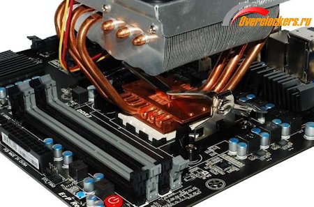
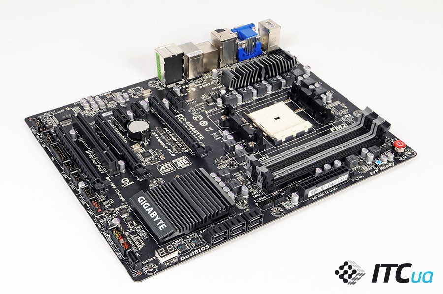
Motherboard Gigabyte GA-F2A85X-UP4
For research Socket platforms FM2 we used the older model in the current line of boards from Gigabyte - GA-F2A85X-UP4 based on the new AMD A85X chipset.


![]()

The board complies with the latest specification Ultra Durable 5 which involves the use of high-quality energy-efficient components. Power stabilizer eight-phase (6+2). The power circuit uses powerful IR3550 assemblies, as well as chokes with ferrite cores. A digital controller is used to control the VRM parameters.
The layout of slots for expansion cards is optimal. Three PCI-E x16, the same number of PCI-E x1 and one PCI. The latter does not require an additional controller, since support for this bus is still implemented in AMD chipsets. Considering the number of PCI Express lanes, the nuances of using slots cannot be avoided. The first slot is set to full speed by default. When using two video cards, the first and second slots are switched to x8+x8 mode. The third full-format PCI-E x16 has a bandwidth of x4, while if the nearest PCI-E x1 is used, then the lower PCI-E x16 will also provide data transfer rates at the x1 level. Gigabyte GA-F2A85X-UP4 allows you to fully realize the advantages of the A85X chipset - the model allows you to create a configuration with two video cards based on AMD chips that will work in CrossFireX mode.
On board Gigabyte GA-F2A85X-UP4 there is a gentleman's set of overclockers - power buttons, Reset, Clear CMOS, and status LED. The board is expectedly equipped with two BIOS chips, and the graphic version of the 3D BIOS is used as a UEFI shell, which is conceptually already well known to us from the manufacturer's previous boards.
Of the interesting features of the model, we note the technology Dual Clock Gen. The board has a microcircuit with an additional clock generator (the main one is in the chipset). According to the manufacturer, it allows you to achieve stable operation at higher bus clock speeds (~135-150 MHz), which may be of interest to owners of APUs with locked multipliers who want to boost their processor. Although, of course, given AMD's pricing policy for Trinity chips, it is better for enthusiasts to initially look towards models with the "K" index.
The board has full set video outputs: DVI, HDMI, DisplayPort and D-Sub. In this case, you can simultaneously connect up to three display devices with any combination of interfaces. Note that the DVI port operates in Dual-Link mode, allowing the use of monitors with resolutions up to 2560×1600.
The disk subsystem will allow you to connect 8 drives via SATA 6 Gb / s: seven internal and one using eSATA. As for the peripherals, the user has six USB 3.0 ports. Four of them are implemented using the chipset, two more use an additional Etron EJ168 controller.
In general, the board leaves a rather pleasant impression. A decent set of features for an older solution, nothing superfluous and at the same time a good start for the future.
Performance
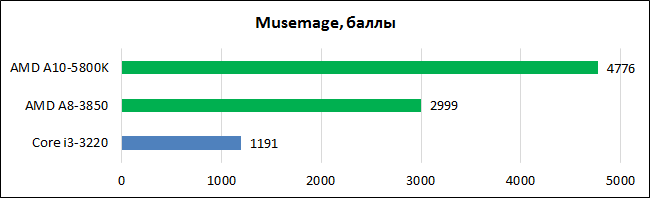
To evaluate the possibilities AMD A10-5800K, we have selected worthy opponents for him. First of all, it's a processor AMD A8-3850. This chip differs from the older model of the previous generation APU line (A8-3870K) only by a 100 MHz lower clock speed and a blocked processor multiplier, while the integrated graphics part is used by the most productive Radeon HD 6550D. From the main competitor, a model of the same price category is presented - dual core processor Intel Core i3-3220
During the test of the new APU, we also decided to evaluate the effectiveness of the bundle CPU+GPU in applied tasks, using for these purposes graphics editor Musemage, which uses the resources of the graphics core to perform various operations. The list of stages included the SVPMark benchmark, which also knows how to connect graphics for video processing.
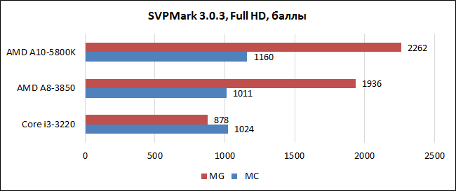
The range of programs interspersed with heterogeneous computing is gradually expanding. Moreover, this is not only synthetic software for tests, but also applied applications. The pace, of course, leaves much to be desired, but there is hope that such developer initiatives will be strongly encouraged by hardware manufacturers. This is the rare case when the interests of both competitors coincide. Intel is also focusing more and more on the performance and capabilities of its integrated video with each successive architectural iteration. The Ivy Bridge chips here have noticeably succeeded in comparison with their predecessors, and in the expected Haswell, the graphics core should receive an even more significant increase in performance. In the meantime, AMD has a much stronger position here.
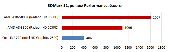
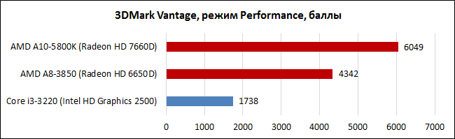
In 3D synthetics, Trinity has a very solid performance increase of 40-45%. Of course, in the overall standings, the increased performance of the x86 block is also taken into account, but this is not bad after all. 6000 points in 3DMark Vantage is almost the level of the Radeon HD 6570, that is, a discrete graphics card, which is now offered for $50-60. The indicators of Intel HD Graphics 2500 look noticeably more modest against the background of "embeddings" from AMD.
Intel offers separate processor modifications equipped with Intel HD Graphics 4000 graphics. In the case of dual-core models of the Ivy Bridge line, this is the Core i3-3225. It also has an operating clock speed of 3.3 GHz, like the Core i3-3220, but is equipped with a full-fledged graphics module with 16 compute units (the HD Graphics 2500 has only six), although it costs $ 20-25 more. At the time of writing, we did not have such a model, however, in order to include in the review not only the results of the Intel HD Graphics 2500, but also the indicators of the most powerful integrated graphics card to date. Intel Solutions, we used Core i7-3770K. It appears only in gaming tests with embedded video. This will allow a more balanced assessment of the current position and potential capabilities of the integrated GPUs of both companies.
Integrated video capabilities are highly dependent on the performance of the memory subsystem. Let's see how in the case of the A10-5800K RAM bandwidth affects gaming performance.
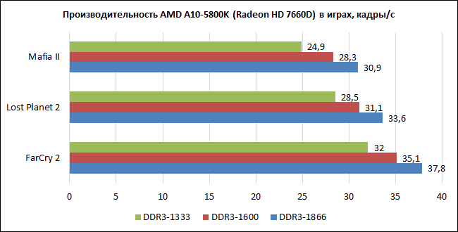
If an integrated video core is used, DDR3-1866 is highly recommended. High-speed or overclocked memory modules to such frequencies will provide an 18-24% increase in performance in games.
Performance with discrete graphics
We also tested discrete graphics platforms using the reference model Radeon HD 7970(925/5500 MHz), which will definitely not become a limiter for processors of this level.
In general, the increase in computing performance of Trinity is relatively small and is on average at the level of 5-15%. Despite the fact that full-fledged Llano computing cores still turn out to be preferable to dual modules in some cases, due to internal architecture improvements, as well as higher clock frequencies, Piledriver-based chips manage to outperform their predecessors. The possibilities of integrated graphics pleased more. A 30% advantage over its predecessor, which before the advent of Trinity was a kind of benchmark in terms of the capabilities of the built-in GPU, inspires optimism.
Energy consumption
Having gained a general idea of the performance of the Trinity APUs, we were also interested in evaluating the power consumption of the new AMD processors. The declared TDP parameter for the A10-5800K is 100 W, let's look at the real performance in typical tasks.
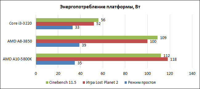
During the load on the computing units (rendering in Cinebench), the consumption of Llano and Trinity is approximately at the same level. But the increase in the power of the graphics core did not go unnoticed. In games where it is the GPU that is more loaded, the power consumption of the A10-5800K is 18 W higher than that of its predecessor. The manufacturing process remained the same, but higher clock frequencies make themselves known. At the same time, it is worth noting that in rest mode, in which the processor is often found most of the time, the energy efficiency of the new APUs is higher. However, here it is worth making an allowance for the fact that different motherboards are used for both processors, which can affect the absolute figures.
Dual-core Intel Core i3 as a whole demonstrate exemplary efficiency. The CPU consumes a minimum of energy for computing tasks, but when evaluating performance in games, it is worth considering a significant difference in the speed of solutions.
Results
Platform Socket FM2 and processors Trinity are quite an interesting option for building sufficiently powerful multimedia PCs. Compared to its predecessors, the performance of Piledriver computing units has not increased as much, while the integrated graphics capabilities have been improved by a third, reaching the performance of entry-level discrete graphics cards. At the moment, this is a serious advantage of AMD solutions. At the same time, the range of Trinity chips is exactly the same as that of Llano. Considering the balanced price, they will look very organically as part of inexpensive universal solutions “for everything”. And although in Lately for such tasks are increasingly purchased mobile systems, new APUs in the desktop version will also find their customers.
Test bench configuration
| CPU |