Architecture Ivy Bridge is a continuation Sandy Bridge. The peculiarity of this difference is expressed in the presence of 22 nanometers. As a result, productivity has increased and energy consumption has decreased. In addition, processors new architecture Other improvements have been added:
Added 16 graphics execution units;
Increased IPC (the number of possible instructions executed per clock cycle);
Improved throughput DDR3 memory controller channel (2800 MT/s);
PCI Express has been updated from 2.0 to 3.0, except for the i3 series;
The 7 series chipsets have been updated with USB 3.0;
The ability to connect not 2, but 3 monitors;
Improved integrated graphics: for a home PC – HD Graphics 2500, it is not much different from previous version(Sandy Bridge), for mobile devices(laptops) – HD Graphics 4000, received high performance performance, outperforming both old models and any new ones from competitors;
Quick Sync (video encoding and decoding) now improves performance 75 percent faster (was only 15 percent in the 2nd generation).
Ivy Bridge tests.
The list doesn't end there. Intel has tried to make as many improvements as possible to the Ivy Bridge architecture. Unfortunately, tests showed a slight difference between the third generation and the second.

In some tasks, productivity increases by about 15 percent. But for ordinary household tasks, the increase ranges from 5 to 10%. And this cannot be called a good indicator.
On a positive note.
Changing the processor will be beneficial for a person if he needs to switch to a more powerful line, for example: from i3 to i5. Or you are not satisfied with the clock frequency, and you decided to take it from the middle segment, but to the maximum. Then this is the case when a processor based on the Ivi Bridge architecture is ideal for you.
Users whose hobby is working with video (encoding) will be pleased with Quick Sync. In this case, it is worth changing the processor. Intel has placed great emphasis in this direction. However, when choosing a processor, do not forget about other processor parameters.

Conclusion.
Expectations were not met. The architecture of the third generation is not much different from the second. And if a person already uses Sandy Bridge, then there is no need to change the processor. However, the processor, which has long been discontinued, can be replaced with the 3rd generation. In addition, purchasing a new product based on Ivy Bridge architecture will suit people for specific tasks.
The inevitability of another change in processor generations Intel Core there was no doubt about it. Representing the highest excellence in Intel processor technology, the third Intel generation Core, formerly known as Ivy Bridge, is already making a significant impact on the embedded market.
ZAO RTSoft, Moscow
Leading manufacturers of hardware for embedded solutions traditionally almost simultaneously with official premiere Intel processors Core third generations presented a lot of products based on them, thereby laying the necessary foundation for the industry’s transition to a new platform. The importance of Intel technologies for the embedded solutions market is now difficult to overestimate. There are, one might say, almost no fundamentally closed segments and niches left for the processors produced by the corporation. And therefore, the premiere of the third generation Intel Core, previously known under the code name Ivy Bridge, simply could not go unnoticed. At the same time, many might have a reasonable question: do the presented processors provide a qualitatively new level of capabilities for developers of embedded solutions? And, accordingly, is it really necessary to switch to them?
The previous, second generation of Intel Core, also known as Sandy Bridge, turned out to be extremely successful in the embedded systems market, and it would be quite disingenuous to say that these processors, which debuted in 2011, are now hopelessly outdated. Moreover, in the embedded systems industry these days it is considered good form to release products with life cycle lasting 5-7 years or more, which is required by many customers (this is especially true for “conservative” markets, which include, for example, the defense complex, transport sector, industry, telecommunications industry, medical field, etc.). New generations of Intel processors, as we know, appear much more often. Whether there is some contradiction here or is it only apparent, opinions differ on this matter.
But in any case, no matter what point of view you lean towards, it is clear that it is necessary to take a closer look at the third generation of Intel Core, evaluate the merits of these processors and their role in the embedded systems market. All this will be discussed below.
Moore's inexorable law
The arrival of the third generation of Intel Core to replace the second was inevitable, like autumn leaves or winter cold. Everyone has long been accustomed to the methodical regular updating of Intel processor product lines in accordance with Moore's Law. This law bears the name of one of the founders of the corporation and the current honorary chairman of the board of directors of Intel and is already known far beyond the borders of the semiconductor industry. There are different interpretations of Moore's Law, but most of them imply a significant improvement in processor characteristics (performance, total number of transistors, transistor density on the chip) over a period of 18 to 24 months. It was first formulated by Gordon Moore in the 1960s not as a law, but as an empirical observation, and has since become a powerful tool for marketing and planning research and development. Skeptics have repeatedly tried to predict the end of its action, but the law works successfully to this day.
Several years ago, Intel made a strategic decision to alternate innovations implemented at the processor microarchitecture level with those associated with the transition to more sophisticated manufacturing technologies. In accordance with this principle, the third generation of Intel Core marks the beginning of the large-scale introduction of 22‑nanometer processor technology using 3D transistors. This is the main, but not the only difference between Ivy Bridge and Sandy Bridge generation processors, made using 32 nm technology using conventional planar transistors.
Improvements in the manufacturing process have made it possible to reduce the die area (160 mm² versus 216 mm² for comparable quad-core Ivy Bridge and Sandy Bridge variants). At the same time, the placement density and the total number of transistors on the chip were increased (1.4 billion versus 1.16 billion in the same example). The power consumption of Ivy Bridge processors has been significantly reduced and their performance has increased compared to Sandy Bridge. In general, according to independent experts, technological innovations have provided the third generation of Intel Core with an overall increase in computing power of approximately 20%, and productivity per watt of electricity consumption of up to 40%.
At the same time, architecturally, the third generation of Intel Core differs slightly from the second. The Ivy Bridge microarchitecture is a derivative of Sandy Bridge. Some differences, of course, are present, but there is no talk of radical innovations like the appearance of AVX (Advanced Vector Extensions) technology in Sandy Bridge processors.
According to experts, it was the support of AVX technology, which supplemented the instruction set of x86‑compatible processors with vector extensions for working with data in floating-point format, that at one time provided the second generation of Intel Core with a brilliant breakthrough in the market of embedded solutions.
From the third generation of Intel Core, unlike the second, no one really expected revolutionary changes in the embedded technology market. Nevertheless, developers of embedded solutions generally greeted the release of Ivy Bridge processors very positively. Why?
Pros of Ivy Bridge and market realities
For some, the increase in computing power of the third generation of Intel Core compared to the second may be modest. It is possible that there will be those who are not particularly impressed by the improvement in energy consumption characteristics. We will not argue about tastes and subjective impressions. But we note that it is hardly advisable to evaluate processors by themselves - in isolation from the systems based on them and the applications for which these systems are intended.
Thus, there is a fairly impressive layer of embedded applications that always require the highest available computing performance, signal processing and graphics operations in combination with the highest possible communication channel bandwidth (defense, medicine, telecommunications). For them, the Ivy Bridge platform today seems to be an excellent choice, since it realizes all the architectural advantages of Sandy Bridge based on more advanced manufacturing technology, providing additional gains in performance and energy efficiency. Let's not forget that this technology made it possible to place a more powerful graphics core on the Ivy Bridge chip, which is capable of including up to 16 actuators (Sandy Bridge has no more than 12) and supports graphical interfaces DirectX 11, OpenGL 3.1, OpenCL 1.1. At the same time, the crystal area, as noted above, did not increase, but, on the contrary, decreased.

Rice. General structure of the embedded platform computer systems
based on third generation Intel Core processors
The communications capabilities of the Ivy Bridge platform are also significantly improved compared to Sandy Bridge. At the processor level, support for up to 16 PCI Express (PCIe) 3.0 lanes is implemented - this technology provides twice the bandwidth compared to PCIe 2.0, allowing, for example, the use of modern high-end video cards in solutions and the use of high-speed interfaces for external communications (including 10GbE and 40GbE).
The integrated third-generation Intel Core memory controller supports the DDR3-1600 specification as standard. It is also capable of working with lower voltage DDR3L devices (1.35V versus 1.5V for regular DDR3 devices), which may be useful when building systems for mobile applications.
Summarizing the above, we note that the markets for embedded computer technology at the moment, they not only do not hinder, but even to some extent are favorable for the potential of using systems based on third-generation Intel Core processors to be fully revealed. Moreover, the previous, second generation created a fairly good foundation for further advancement. Therefore, the enthusiasm with which leading manufacturers began to replenish their product lines with products based on Ivy Bridge processors was understandable. We'll talk about some of these products in more detail.
VPX: on the way to new heights
The thesis that the VPX system architecture is one of the best platforms for creating secure multiprocessor systems based on x86‑compatible processors can be considered almost undeniable today. Those who doubted this seem to have been finally convinced by the success of VPX solutions with Sandy Bridge processors in the systems markets for defense and aerospace applications.
The Ivy Bridge generation is accordingly tasked with consolidating the successes achieved by its predecessors and, where possible, building on them. An important role in solving this problem belongs to Intel's partners - leading manufacturers of hardware for embedded systems, one of which is Kontron. For VPX systems in the 3U form factor, Kontron offers the VX3042 modules (standardly based on a dual-core Intel Core i7-3517QE with a nominal clock frequency 1.7 GHz and configurable TDP) and VX3044 (with quad-core Intel Core i7-3612QE/2.1 GHz). The first is intended primarily for consoles and rugged combat servers oriented to harsh operating conditions. The second involves use as part of high-performance computing clusters.
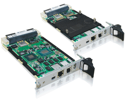
Rice. Kontron VX3042 (top) and VX3044 VPX boards
support proprietary Kontron VXFabric software technology
Both products comply with the OpenVPX (VITA 65) and VPX REDI (VITA 48) standards and are available to customers in three versions depending on the operating temperature conditions and the cooling system used. The boards support intra-system communications using PCIe 3.0 and 10GbE buses, as well as Kontron’s proprietary technology called VXFabric, which implements IP data transfer over PCIe channels. Front I/O is provided by mini DisplayPort, Gigabit Ethernet, USB 2.0 and serial interface connectors (RS‑232 or RS‑485).
COM Express (PICMG COM.0) products, which traditionally embody the most advanced technological advances in the field of small-sized embedded systems, are rightfully considered by many experts to be one of the main driving forces of the rapid growth of the COM solutions industry that we are currently witnessing. As expected, the leading manufacturers of these products greeted the third generation of Intel Core fully armed and quickly prepared the corresponding products for launch on the market. Thus, the Kontron company, which is the founder this standard, soon introduced two new series of COM Express modules in the basic form factor based on Ivy Bridge processors - COMe bIP2 (with Type 2 pinout) and COMe bIP6 (Type 6).
The models of these series differ primarily in the type of processor used. This can be a dual- or quad-core processor of the Intel Core i3-3000, Intel Core i5-3000 or Core Intel i7-3000 family (modified for embedded mobile applications) with a clock frequency of 1.6 to 2.7 GHz and a thermal package of 17 up to 45 W.
Allowing the ability to simultaneously output independent video streams to three displays, all COMe bIP2 and COMe bIP6 modules support three DisplayPort display interfaces (can be used with DVI monitors and HDMI - using adapters), including one eDP (DisplayPort option for embedded applications). If necessary, you can also use the SDVO port, dual-channel LVDS interface, or analog interface for connecting CRT monitors with a resolution of up to 2048x1536 to output a video stream.
The capabilities of the presented modules for working with disk drives include support for two third-generation SATA devices (bus bandwidth - 6 Gbit/s) and two similar second-generation devices (3 Gbit/s). Modules with Type 2 connector also allow the use of one disk drive with parallel ATA interface.
To a somewhat greater extent, the options for supporting PCI, PCIe and USB interfaces depend on the type of module. Thus, Type 2 modules allow the use of eight USB 2.0 ports, a PCIe x16 graphics port, five PCIe x1 lanes and a parallel PCI bus version 2.3 (33 MHz). Type 6 modules have four USB port 3.0, the same amount – USB 2.0, and the number of PCIe x1 lanes is seven. Support for connections via the PCIe x16 bus is also present, but the ability to use a parallel PCI interface is missing.
The communication subsystem of both types of modules includes a Gigabit Ethernet interface. We also note the presence of an integrated cryptoprocessor made in accordance with the TPM (Trusted Platform Module) specification version 1.2, support for ACPI 3.0 technology (implements configuration and power management mechanisms using OS tools) and the use of solid-state capacitors with a tantalum anode, which have increased reliability.
CompactPCI: evolution continues
Among the new 3U CompactPCI processor boards, we note the Kontron CP3003‑SA board. Base configuration options for this product include an Intel Core i7-3517UE, Intel Core i7-3555LE, or Intel Core i7-3612QE processor. The CP3003‑SA board is based on the Mobile Intel QM77 chipset and is available in single-slot (4HP) and dual-slot (8HP) versions. For the 4 HP version, it is optionally possible to install a NAND flash memory module with a capacity of up to 32 GB. From the front panel of the board in this modification, a VGA connector and two USB 2.0 and Gigabit Ethernet connectors are available.
The two-slot version of the board requires the use of one of two proposed expansion module options – CP3003‑HDD or CP3003‑XMC. The first of them provides support for CFast flash cards and 2.5‑inch hard drives and SSD devices. The use of this module also allows you to increase the number of connectors for external connections accessible from the front panel.
The CP3003‑SA board can be installed in either a system or peripheral slot. In the first case, a 32-bit CompactPCI interface is used, operating at a frequency of 33 MHz (optional - 66 MHz). When installed in a peripheral slot, PCI passive mode support isolates the board from the CompactPCI bus.
For 6U CompactPCI systems, GE Intelligent Platforms offers the XCR15 processor module. In terms of its characteristics, this product is largely similar to the previously mentioned SBC625 VPX module - the same processors in basic configurations, the same chipset, the same five versions for use with air or conduction cooling.
The XCR15 processor module is made in accordance with the PICMG 2.16 standard, that is, it can be used as part of CompactPCI systems based on packet switching backplanes. Among other product characteristics, we note the presence of an integrated IPMI 2.0 controller. Also supported various options for connecting PMC and XMC expansion cards.
As main software platforms for the reviewed Kontron and GE Intelligent Platforms devices the OS appears Windows family, and Linux versions and VxWorks. It is clear that the adaptation of other popular software platforms such as QNX, LynxOS, RTX, Integrity, etc. for solutions on Intel platform Core 3rd generation is also a matter of short time.
The fruits of a long-term strategy
In-house development of embedded motherboards, which includes careful component selection and an extensive laboratory testing program, is a long-term strategic priority for Kontron and several other leading players. The Kontron KTQ77/Flex FlexATX motherboard, designed for systems based on dual- and quad-core 3rd generation Intel Core processors, is part of the product range with a seven-year life cycle.

Rice. KTQ77/Flex motherboard in FlexATX form factor
is one of the Kontron products with a seven-year life cycle
The board is based on the Intel Q77 chipset, and its capabilities for connecting expansion cards include two PCIe x16 slots (one for PCIe 3.0 devices, the other supports PCIe second generation specifications and operates in x4 mode), two PCI slots (32 bit, 33 MHz ) and one Mini PCIe connector. To connect drives, six SATA connectors can be used (RAID arrays of levels 0, 1, 5 and 1+0 are supported) and one mSATA connector. External connections are provided by four USB 3.0 connectors, two by USB 2.0 (if necessary, their number can be increased to ten), three by Gigabit Ethernet (RJ‑45), two by DisplayPort, one each by RS‑232 (DB9) and VGA. Optionally, it is possible to install a TPM 1.2 cryptoprocessor.
Another new Kontron motherboard for systems based on Ivy Bridge processors, also related to products with a seven-year life cycle, is called KTQM77/mITX. This device made in the Mini-ITX form factor based on the Mobile Intel QM77 chipset and is somewhat different from the KTQ77/Flex in terms of the ability to use expansion cards and connect external devices. Thus, the PCIe x16 slot with support for PCIe 3.0 on the KTQM77/mITX board is adjacent to the PCIe x1 connector for second-generation PCIe devices; there is no possibility of installing devices with a parallel PCI interface at all, and two Mini PCIe connectors are located with reverse side fees. To connect monitors, two DisplayPort connectors and one DVI connector can be used. At the same time, the ability to use USB devices, SATA drives (including RAID support) and network connections KTQM77/mITX are completely similar to KTQ77/Flex. And if necessary, an option with a data encryption module that complies with the TPM 1.2 specification can also be implemented.
VME: “veteran” remains in service
One of the long-lived leaders of the embedded technology market, the VMEbus architecture, recently celebrated its 30th anniversary and has no plans to retire. VME solutions continue to hold a fairly strong position in the segment of defense and aerospace applications, and are receiving worthy additions in the form of products based on Ivy Bridge processors.
The XVR15 processor module from GE Intelligent Platforms is almost a twin of the XCR15 discussed above and, accordingly, is in many ways similar to the SBC625. The XVR15 board is designed for 6U VME systems and is based on the system logic Mobile Intel QM77.
If you take a closer look at the design of these two boards, of course, you can find some differences, and not only due to the architectural features of the CompactPCI and VME standards. But at the same time, the similarities in characteristics are, as they say, striking - identical design options for various cooling systems and temperature ranges, support for software platforms, etc.
In general, we see that for systems based on similar backbone-modular standards, GE Intelligent Platforms offers processor boards based on Ivy Bridge, similar in their characteristics, basic configurations and design options. There is certainly logic in this. Customers representing the defense and aerospace industries are known for their conservatism, which is reflected, in particular, in the choice of backbone-modular architectures used. GE Intelligent Platforms' approach is to not try to influence this choice, but to give the customer the opportunity to get a solution made using the most advanced technologies in any case.
AMC: for telecommunications and more
The market for AMC (Advanced Mezzanine Card) processor modules used in AdvancedTCA and MicroTCA systems is one of those whose growth even the global economic recession could not prevent. By 2015, according to analysts, this market could grow more than two and a half times compared to 2010, and the current generation of products like the Kontron AM4022 obviously has to play a key role in this.
The AM4022 board is based on the Mobile Intel QM77 chipset and is equipped as standard with an Intel Core i7-3555LE or Intel Core i7-3612QE processor (others are also available upon customer request). Supports up to 8 GB of DDR3-1600 ECC memory and up to 64 GB of SATA flash storage.
The communications capabilities of the AM4022 processor module include support for in-system PCIe interfaces (in x4 and x8 configurations) and Gigabit Ethernet, ensuring compatibility with MCH controllers such as Kontron AM4901 and AM4904. From the front panel, two external network connections Gigabit Ethernet (RJ‑45), one USB 2.0 connector and one more – DisplayPort or RS‑232 (10‑pin mini-connector). We also note the presence of an integrated MMC (Module Management Controller) controller with support for intelligent control IPMI 2.0 and the optional ability to use the TPM 1.2 cryptoprocessor.

Rice. Processor module Kontron AM4022
made on the Mobile Intel QM77 chipset and in a standard configuration
equipped with an Intel Core i7-3555LE or Intel Core i7-3612QE processor
The standard version of the AM4022 module assumes operation at temperatures from –5 to +55 °C. Available in modifications that support an extended temperature range – from –40 to +70 °C. At the customer's request, the front panel of the module can be made in accordance with the MTCA.1 standard, which makes it possible to use the device as part of protected outdoor and mobile air-cooled MicroTCA systems.
Among the software platforms for which support for the AM4022 module was implemented in the first place, we highlight, in particular, Windows 7 and Windows Server 2008 R2 and also Red Hat Enterprise Linux and Fedora. The main area of application for AMC modules is still telecommunications applications, and the Kontron product is no exception in this sense. However, MicroTCA solutions using AM4022 boards can also be used in areas such as medical, aerospace and defense, test and measurement devices, security systems, etc.
Software environment: it definitely hasn’t gotten any worse
Software support for new generations of processors is another traditional issue, which, however, is addressed not only and not so much to Intel, but to its partners.
With regard to application software, the issue of optimization for the Ivy Bridge platform is obviously less pressing than it was in the case of the previous generation - Sandy Bridge. The reason is that at the microarchitecture level these processors differ little from each other. In fact, for many applications, optimization for new processors is optional. Yes, the third generation of Intel Core added several AVX instructions. Compared to the original implementation of this technology in the Sandy Bridge microarchitecture, the step forward taken is very positive, but not so great.
Ivy Bridge processors also have new security features - Intel Secure Key (includes a digital random number generator used to enhance cryptographic algorithms) and Intel OS Guard (provides a mechanism for blocking software attacks from user-mode applications when the system is running at the maximum privilege level). And it is no coincidence that among the software developers for embedded solutions that responded to the premiere of Ivy Bridge, one of the most notable newsmakers, again, as at the launch of Sandy Bridge, was LynuxWorks, which announced the release of a version of the LynxSecure secure virtualization package optimized for the presented platform.
Note that for the second generation Intel Core, despite all its architectural innovations, many among specialists did not consider software support to be a matter of paramount importance, and such a point of view was not without foundation. Without going into a debate on this issue, we will limit ourselves to the following statement: in terms of software support, the current position of Ivy Bridge is at least no worse than what Sandy Bridge had in its time.
Conclusion
To summarize, we once again emphasize that third-generation Intel Core processors combine the architectural advantages of the previous, second generation with the advantages of switching to a more refined technological process, expressed in further increases in performance and energy efficiency. Raising the bar even higher in the next evolution of embedded systems, the Ivy Bridge platform is now and in the near future the logical choice for a wide range of embedded applications targeting a variety of vertical markets.
HELL. Sysoev, director of the department,
CJSC "RTSoft", Moscow,
tel.: (495)967‑1505,
Architecture Features
For several years now, the release of new generations of Intel processors has been subject to the empirical TICK-TOCK rule, the essence of which is that the transfer of production to a new technological process(TICK) and the introduction of a new processor microarchitecture (TOCK) occur alternately at intervals of two years. For example, if in the first year there is a transition to a new manufacturing process, then in the second year a new processor microarchitecture is introduced using the same manufacturing process. And the next year the microarchitecture is transferred to a new production process.
Last year, Intel released 32nm Sandy Bridge processors based on a new microarchitecture (TOCK cycle). In April, the company announced a 22nm version of processors based on the Sandy Bridge microarchitecture, which were codenamed Ivy Bridge (TICK cycle).
However, Ivy Bridge processors are not just a 22nm version of Sandy Bridge processors. In this case, we are talking about a significant modernization of the microarchitecture itself. That is why Intel calls this transition to a new process technology not just a TICK cycle, but a TICK+ cycle.
We have already written about the new Ivy Bridge processors on the pages of our magazine, however, it seems to us that the official announcement of these processors is such a significant event that it makes sense to repeat something and compile in one article all those available on this moment information about these new processors.
So let's look at how Ivy Bridge processors differ from Sandy Bridge and why the new processors are not just a 22nm version of the previous generation processors.
The Ivy Bridge processor, like the Sandy Bridge processor, has an integrated PCI Express controller with 16 lanes. However, if in the case of the Sandy Bridge processor we were talking about a PCI Express 2.0 controller, then the Ivy Bridge processors use a PCI Express 3.0 controller.
The difference in throughput between PCI Express 2.0 and 3.0 interfaces is quite significant. Thus, for the PCI Express 2.0 interface, the throughput of each line in each direction is 500 MB/s, and for the PCI Express 3.0 interface - 1 GB/s. It is easy to calculate that for the PCI Express 3.0 x16 interface the throughput is already 32 GB/s.
Of course, to implement the capabilities of the PCI Express 3.0 interface in the Ivy Bridge processor, you also need a video card with a similar interface. However, even in this case, you should not expect that using the PCI Express 3.0 interface will improve system performance in games. As tests show, the PCI Express 2.0 interface is not a bottleneck for modern games and switching to a faster interface will do nothing.
The Ivy Bridge processor, like the Sandy Bridge processor, has a built-in dual-channel DDR3 memory controller. However, in the Ivy Bridge processor it supports faster and lower voltage (1.35 V) memory.
The most important difference between Ivy Bridge processors and Sandy Bridge is that they are manufactured using a 22-nm process technology (Sandy Bridge processors are manufactured using a 32-nm process technology), that is, the geometric dimensions of the transistors will be 1.45 times smaller. Naturally, this affects all characteristics of the transistor.
The main problem associated with reducing transistor size is that an exponential increase in the number of transistors on a chip leads to an exponential increase in power consumption and, as a result, overheating of the chip. The reason for this negative phenomenon is that reducing the size of the transistor leads to leakage currents. In particular, when the thickness of the dielectric layer is reduced to a value of several nanometers, the effects of charge tunneling through the dielectric layer begin to occur, which leads to the appearance of leakage currents.
Planar and Tri-Gate transistors
This problem is partially solved by using, instead of silicon dioxide, which has been used for many years as a dielectric in transistors, other dielectric materials that make it possible to obtain thicker dielectric layers, but which nevertheless provide an increase in the capacitance of the gate capacitor. Such materials must have a higher dielectric constant, and therefore are called High-K dielectrics. It is clear that the use of alternative materials with a higher dielectric constant makes it possible to increase the thickness of the dielectric layer, which, in turn, reduces leakage currents.
That is why, starting from the 45-nm manufacturing process, transistors with High-K dielectrics (High-K/metal gate) are used in the manufacture of processors.
Of course, the use of High-K dielectrics is just one of the improvements that planar transistors have undergone. You can also recall strained silicon technology, which began to be used in the manufacture of NMOS and PMOS transistors using the 90-nm process technology to improve their performance characteristics. The voltage generation technology allows increasing the mobility of both electrons and holes and increases the switching speed of transistors.
The latest revolutionary improvement in the structure of field-effect transistors concerns a fundamental change in their geometry - transistors have turned from flat to three-dimensional.
The development of three-dimensional transistor designs began back in 2002. In September 2002, Intel announced the development of a three-dimensional triple-gate transistor design (Tri-gate), which provides more efficient power consumption compared to traditional planar transistors.
The 3D triple gate transistor is based on a 3D structure that looks like a raised horizontal plane with vertical walls.
This structure allows electrical signals to be sent both along the “roof” of the transistor and along both of its “walls”. In fact, it is as if there is not one shutter, as in a planar structure, but three at once (two walls and a lid). Hence the name - “triple gate” (Tri-gate).
Thanks to such a current distribution scheme, the area available for current passage effectively increases, and therefore its density and, along with it, the leakage current decreases. The triple gate is built on an ultra-thin layer of fully depleted silicon, which further reduces leakage current and allows the transistor to turn on and off faster while significantly reducing power consumption.
A feature of this design is also the raised source and drain - as a result, the resistance is reduced, which allows the transistor to operate at a lower power current.
Despite the fact that the development of the three-dimensional design of transistors began back in 2002, their use in the production of processors became possible only almost 10 years later, that is, with the transition to a 22-nm manufacturing process.
3D Tri-Gate transistors, manufactured on a 22nm process technology and operating at low voltage, provide up to 37% more high performance in comparison with conventional transistors made on the basis of 32 nm technology. Processors with the new transistors can consume less than half the power of 32nm 2D chips while maintaining the same level of performance.
We also note that Intel was the first to use three-dimensional transistors in the production of microcircuits. All other chip companies will be able to start producing 3D transistors in no earlier than four years.
So, one of the main innovations in 22nm Ivy Bridge processors is the use of more productive and energy-efficient three-dimensional Tri-Gate transistors. However, this is not the only difference between 22nm Ivy Bridge processors and 32nm Sandy Bridge processors.
As for the computing core of the Ivy Bridge processor, it has not undergone architectural changes in comparison with the Sandy Bridge computing core. But the integrated graphics core with support for DirectX 11, codenamed Carlow, is indeed one of the main innovations in the Ivy Bridge microarchitecture.
According to the application Intel, the graphics core in Ivy Bridge processors will be 60% more productive than the graphics core in Sandy Bridge processors.
In addition to support for DirectX 11, the Carlow graphics core will support OpenGL 3.1 and OpenCL 1.1, that is, graphic Intel core will be able to perform calculations using shader processors.
Let us recall that in the Sandy Bridge processor the graphics core contains (depending on the processor model) six or 12 execution units (Execution Unit, EU), each of which has one texture unit. In the Ivy Bridge graphics core, the maximum number of execution units has been increased to 16, with each execution unit already having two texture units.
Blocks for hardware tessellation and Shader Array support were also added to the Ivy Bridge graphics core (which, in fact, made it possible to achieve compatibility with Shader Model 5.0 and DirectX 11).
It is interesting to note that the GPU clock speed of the Ivy Bridge processor is lower than the GPU clock speed of the Sandy Bridge processor, which helps reduce power consumption. As a result, in terms of performance per watt, the Carlow graphics core is twice as powerful as the HD 2000/3000 core in the Sandy Bridge processor. Note that there will be two implementations of the Carlow graphics core - HD 4000 and HD 2500, which differ from each other in the number of functional blocks.
The changes also affected Intel Quick Sync technology. First of all, the manufacturer promises a twofold increase in the speed of HD video transcoding using specialized processor units. In addition, an improvement in encoding quality and the addition of the ability to apply filters such as improving color gamut or contrast to the transcoded video stream are announced.
The power of the hardware video decoder will be enough to simultaneously play back at least 16 HD video streams. Another innovation in Ivy Bridge processors is configurable TDP.
Let us recall that TDP is one of the most important characteristics of Intel processors. In particular, the TDP value determines both the maximum power consumption of the processor and the required efficiency of the cooling system. The TDP value is also tied to the ability to increase the clock frequency of processor cores in Turbo Boost mode (that is, the clock frequency can be increased only if the TDP value is not exceeded or this excess is short-term).
Ivy Bridge processors have not one, but three TDP values: minimum, nominal and turbo. That is, with sufficient heat dissipation, the TDP of the processor can be increased and its clock frequency in Turbo Boost mode will accordingly increase. If you need to reduce power consumption as much as possible, then TDP can be reduced.
It is clear that configurable TDP technology is aimed primarily at mobile processors. So, if the laptop is powered from the network and sufficient cooling of the processor is provided, then the TDP can be increased. If the laptop works in offline mode, then in order to increase the time battery life It is advisable to reduce the TDP of the processor.
It is important to note that Configurable TDP technology does not replace Intel Speed Step technology or the choice of processor power consumption scheme in the operating system settings. It only complements all the technologies that already exist.
Significant improvements have been made in terms of overclocking Ivy Bridge processors. Let us recall that in Sandy Bridge processors with an unlocked multiplier (K-series processors) the maximum multiplier was 57. That is, even theoretically, Sandy Bridge processors could not be overclocked above a frequency of 5.7 GHz (Sandy Bridge processors are almost impossible to overclock by increasing system bus frequency). In Ivy Bridge processors, the maximum multiplier factor is increased to 63, that is, by changing the multiplier factor, the processor can theoretically be overclocked to a frequency of 6.3 GHz.
Another innovation in the overclocking capabilities of the Ivy Bridge processor is the ability to change the multiplier without having to reboot the system.
The next innovation in the Ivy Bridge processor is the presence of a hardware random number generator (Digital Random Number Generator, DRNG), which is used in cryptographic tasks. In general, random number generators have been used in processors for a long time. However, so far we have been talking about pseudo-random generators that operate in accordance with a certain mathematical algorithm. The Ivy Bridge processor uses a real (not pseudo-random) random number generator, which is based on an electronic circuit with an indeterminate state, which allows it to generate a stream of random characters in 16-, 32-, or 64-bit format at a speed of 2 or 3 Gbps.
Innovations also include the Supervisory Mode Execute Protection (SMEP), which is an implementation of technology to protect against elevation of privileges. This technology controls the level of privileges of the executable code, which is located in the address space allocated for work by programs (Applications). In fact, the classic attack aimed at escalating privileges and necessary to gain access to system resources is blocked at the hardware level.
Ivy Bridge processor lineup
Intel is going to release a fairly impressive range of Ivy Bridge processors, which will be represented by the Intel Core i7, Core i5 and Core i3 families (Table 1). These processors will differ in clock speed, graphics core version (HD 4000 or HD 2500), number of cores (four or two), support for Hyper-Threading technology, L3 cache size and TDP. All Ivy Bridge desktop processors feature an LGA 1155 processor socket and are compatible with boards based on Intel 7-series chipsets, and in some cases, boards based on Intel 6-series chipsets.
All processors of the Intel Core i7 family are quad-core and support Hyper-Threading technology. The L3 cache size for them is 8 MB, they have an integrated HD 4000 graphics core with a base clock speed of 650 MHz, which can be increased to 1150 MHz in Turbo mode.
The Intel Core i7-3770K processor is the top model in the Intel Core i7 family. It differs in that it has an unlocked multiplier (indicated by the letter “K”) and is aimed at fans of extreme overclocking. However, its TDP is only 77 W.
In general, if the letter “K” appears in the name of the processor, this means that it has an unlocked multiplier. The absence of a letter is the base model of the processor. For base models and K-series processors of the Intel Core i7 and Core i5 families, the TDP is 77 W. Well, for basic models of processors of the Intel Core i3 family, TDP is 55 W.
The presence of the letter “S” means that the TDP level is 65 W, and the letter “T” means that the TDP is 45 W for quad-core processors and 35 W for dual-core processors.
A distinctive feature of the Intel Core i5 family of processors is the presence of four logical cores. That is, these can be quad-core processors without support for Hyper-Threading technology or dual core processors with support for Hyper-Threading technology. More precisely, all, with the exception of one, processors of the Intel Core i5 family are quad-core, but do not support Hyper-Threading technology. The L3 cache size for these processors is 6 MB. And only one model in the Intel Core i5 family is dual-core. This is about Core processor i5-3470T. It supports Hyper-Threading technology, and therefore, like all other processors of the Intel Core i5 family, is recognized by the operating system as quad-core (four logical cores).
All processors in the Intel Core i5 family have an HD 2500 graphics core with a base clock speed of 650 MHz and 1050 MHz in Turbo mode. The only exceptions are processors with a number ending in “5” (for example, Intel Core i5-3475S). These are processors with HD 4000 graphics core.
The distinctive features of the Intel Core i3 family of processors include, firstly, the fact that they are all dual-core and do not support Hyper-Threading technology, that is, from the point of view operating system are dual-core, and secondly, these processors do not support Turbo mode for processing cores.
If the processor label ends with the number “0,” this means that the processor has an HD 2500 graphics core, and if it ends with the number “5,” it means that the processor has an HD 4000 graphics core.
Intel 7 Series Chipsets
The new Intel 7-series chipsets are also designed for the new Ivy Bridge processors. As noted, Ivy Bridge processors are compatible with boards based on Intel 7-series chipsets, and in some cases, with boards based on Intel 6-series chipsets. That is, it is possible that in order for the Ivy Bridge processor to work on a board with an Intel 6-series chipset, a BIOS flashing will be required, and perhaps the Ivy Bridge processor will under no circumstances work on a board with an Intel 6-series chipset. In a word, before taking any risks, you need to familiarize yourself with the list of processor models supported by the board.
Note that a similar situation is observed with Sandy Bridge processors. They may or may not, as our experience shows, start up with boards based on Intel 7-series chipsets. Moreover, this is despite the fact that formally all Sandy Bridge processors must be compatible with boards based on Intel 7-series chipsets.
However, let's return to the Intel 7-series chipsets. Actually, motherboards based on Intel 7-series chipsets went on sale even before the announcement of the Ivy Bridge processor, which, in principle, is logical, since these boards are fully compatible with Sandy Bridge processors. The only exception is Intel chipset X79 Express, which was announced a long time ago. It also belongs to the 7 series of Intel chipsets, but stands apart because it is only compatible with Sandy Bridge-E processors with an LGA 2011 socket. Accordingly, we will not consider it in this review. All other Intel 7-series chipsets are only compatible with processors with the LGA 1155 socket.
A distinctive feature of the new Intel 7-series chipsets is support for USB 3.0 and SATA 6 Gb/s ports.
The most widespread chipset will be for desktop processors Intel Z77 Express, which is aimed at high-performance and mass-market PCs. It supports processor graphics, has eight additional PCI Express 2.0 lanes, supports ten USB 2.0 ports and four USB 3.0 ports, as well as four SATA 3 Gb/s ports and two SATA 6 Gb/s ports. In addition, the Intel Z77 chipset supports Intel Smart Response Technology and allows you to overclock the processor. This chipset makes it possible to implement three configuration options for PCI Express slots through 16 PCI Express 3.0 lanes supported by the Ivy Bridge processor. This can be only one PCI Express 3.0 slot operating in x16 mode, or two PCI Express 3.0 x8 slots, or one PCI Express 3.0 x8 slot and two PCI Express 3.0 x4 slots.
The Intel Z75 chipset has more modest capabilities. It also allows you to overclock the processor, but does not support Intel Smart Response Technology. In addition, this chipset allows for only two configuration options for PCI Express slots. This can be only one PCI Express 3.0 slot operating in x16 mode, or two PCI Express 3.0 x8 slots.