Greetings, my dear readers. The subject of our conversation today will be register memory. Most of you are probably hearing this term for the first time, since ordinary user computers have nothing to do with it. And if so, then it is logical to assume that such a module has some additional or extraordinary capabilities.
We are talking about a type of RAM, and you will say that it would be nice to get it and try it out. But let's not rush. Read the article to the end and you will find out not only what kind of memory this is, but also what you can and cannot do with it.
First, let's define the terms.
Registered Memory is abbreviated RDIMM, as it is a type of regular DIMM memory, which we know well as DDR2, DDR3, DDR4.
Accordingly, non-registered memory is called unregistered DRAM or UDIMM. Register memory is also called buffer memory, which is true regarding the principle of its operation.

What are registers for?
Now let's remember how RAM works. Data is loaded into it from the hard drive, but commands to perform these actions come from the central processor. Or rather, from the memory controller, which is directly connected to the RAM chips. When ordinary computers (even gaming ones) operate, all processes occur as normal.
But on servers, the intensity of access to the RAM is much higher, and many unrelated requests can be processed simultaneously. Obviously, in this case, several RAM chips can be used at once, which leads to an increase in the current load on the controller and increases the risk of its failure.
To increase the reliability of the “RAM – Controller” system, a register module is integrated between them, in which information is pre-buffered when it is read or written. This chip itself is located directly on the RAM strip, which is therefore called register memory.

How to identify RDIMM?
It turns out that register memory differs from regular memory in an additional chip, you ask? Of course yes, but don't rush into counting chips.

The fact is that register memory is used exclusively as server memory. This means that it must implement ECC (error-correcting code memory) technology, the purpose of which is to correct errors in information read from RAM. A special processor, also installed on the RAM chip, checks it with the original data recorded in memory, and is able to detect a bit mismatch in one machine word.
Typically, for 8 RAM chips there is one ECC module and one register module, which, by the way, is smaller in size. Knowing this, with a quick glance at the memory bar you can calculate the total number of chips and conclude whether it is a regular RAM or not.

In order not to get confused in counting microcircuits, I still suggest paying attention to the markings, by which you can easily identify the register memory. Just read what it says at the end: if there are "R" or "REG" symbols, then this is it.
Unusual qualities of register memory
Now let's talk about the features of register memory. This is useful information, especially for those who wish to upgrade their PC with it:
An additional buffer element in the communication structure between the RAM and the controller affects the performance of the memory, because each access to the registers is performed clockwise. This means that such memory will be slower than usual by the clock cycle. Compared to SDRAM, the delay occurs for the initial request cycle.
- I already said that register memory is intended exclusively for working on servers. To be more precise, on motherboards designed for them. Therefore, do not try to blow it onto a regular motherboard. Although, if the “mother” supports this possibility (and this can be clarified in her passport), then why not. Again, if your PC functions as a server or is used for remote work, this decision to add reliability is completely justified.
- The main advantage of register memory is increased efficiency of the controller with multiple RAM modules. With RDIMM, you get a scalable system that, with proper processor support, can operate in three or four channel modes. And this is a significant increase in data reading speed and performance (although it is necessary to reduce the operating frequency of the RAM). In practice, this is perfectly implemented in server motherboards like SuperMicro X9DR3-LN4F+, where you can use all 24 RAM slots.

- When planning to increase the amount of memory for multi-channel mode, remember that the joint operation of RDIMM and UDIMM modules is not only impossible, but also unacceptable. So it’s better to immediately select analogues for the existing register memory with the same volume, frequency, etc.
This is what it is, register memory.
Like it or not, it's not for everyone. Yes, it is more expensive and is not on sale so often. But most importantly, it has a narrow server specialization. But, friends, you must agree that RDIMM is a very interesting object, by studying which you will not only increase the level of your computer knowledge, but also receive additional information about the operation of RAM.
With this I end our conversation and wish you all prosperity and success.
Annotation: The principle of operation of registers as elements of electronic memory is considered.
The register is an IC with a medium degree of integration, designed to remember and store a multi-bit word.
Latch register
simplest register is a parallel connection of several triggers (Fig. 8.1a). The UGO of the latch register is shown in Fig. 8.1, b. If register built on latching triggers, it is called register-"latch". Typically, the register IC includes buffer amplifiers and control elements, such as those shown in Fig. 8.2, a. Shown here is the functional diagram of an 8-bit D- latch register KR580IR82 with three output states. Its UGO is shown in Fig. 8.2, b.
Rice. 8.1. Four-bit latch register with direct outputs: a - functional diagram; b - UGO
The third state(the first two are logical 0 and logical 1) is the state of the IC outputs in which they are disconnected from both the power source and the common point. Other names for this condition are high resistance, high impedance state, Z-state[ , With. 61 - 63; , With. 68 - 70].
This is achieved third state special circuit solution [, p. 117 - 118] in the output part of the logic elements, when the output transistors of the logic elements are locked and do not supply either supply voltage or ground potential (not 0 and not 1) to the output.
Register KR580IR82 consists of 8 functional blocks (Fig. 8.2, a). Each of them includes D-latch trigger with falling edge recording and powerful 3-state output valve. STB- strobe input, - transmission permission - signal that controls the third state: if , then information is transferred from the inputs to the corresponding outputs, if , all outputs are transferred to the third state. When and, the IC operates in bus driver mode - information from the inputs is transmitted to the outputs unchanged.
When applying for trailing edge of signal the transmitted information is “latched” into the triggers, that is, what was there at the time of submission is remembered there ![]() . Bye, buffer register will store this information, regardless of the information on D-inputs. When a leading edge is applied
. Bye, buffer register will store this information, regardless of the information on D-inputs. When a leading edge is applied ![]() when saving, the state of the outputs will change in accordance with the change at the corresponding inputs. If , then all output amplifiers are transferred to the third state. In this case, regardless of the state of the inputs, all outputs register are transferred to the third state.
when saving, the state of the outputs will change in accordance with the change at the corresponding inputs. If , then all output amplifiers are transferred to the third state. In this case, regardless of the state of the inputs, all outputs register are transferred to the third state.
All register pins can have an active zero level, which is displayed on the UGO in the form of inverse signals and pin designations.
There are many varieties registers, for example, shift registers [, Chapter 8], in which flip-flops are interconnected in such a way that they transmit information sequentially from one flip-flop to another [, pp. 109 - 122], but here we will focus on the latch register and its application.
Register memory
Register memory - register file - is a super-random access memory (SRAM) - a circuit of several registers designed to store several multi-bit words.
In Fig. 8.3 shows an example implementation SRAM, consisting of four 8-bit registers(connection of RG2 and RG3 is not shown, it is carried out in the same way). Given SRAM has an information volume of 4x8 bits - 4 words of 8 bits, or 4 bytes. Here DI - data input- input data bus, DO - data output- output data bus, WR- write signal to SRAM, R.D.- signal for reading information from SRAM, VSD - internal data bus.
Every register has a two-bit address, which is supplied to the decoder inputs. For example, the leftmost one in Fig. 8.3 register RG1 has the address , next - (not shown in the figure), next - (not shown), and the one on the far right register RG4 has the address .
If there is an active recording signal, the decoder, in accordance with the address code, issues one of registers active signal, which carries information from the input data bus D.I. is recorded in the selected register. On the trailing edge information in this register"snaps"
If, for example, on D.I. information and address provided register is equal to , then the active signal at output “3” of the decoder will be applied as to register RG4. The remaining registers will have an inactive signal level at this time, so information from the input data bus will be written to RG4, and the previously recorded information will be stored in the remaining registers.
When the read signal is active, all 8 multiplexers are activated (the diagram shows the first, second and eighth, the rest are connected similarly), since an active signal is applied to their enabling inputs. In accordance with the filing on address decoder, multiplexers switch information from the selected register to the output data bus. For example, , the register address is . Then at all multiplexers it will be, they all begin to select information in accordance with the address. Therefore, to the output bus DO bits of the internal bus with numbers 25 will be supplied from the first multiplexer, 26 from the second, 27 from the third, 28 from the fourth, 29 from the fifth, 30 from the sixth, 31 from the seventh and 32 from the eighth multiplexer. Thus, information that is a copy of the content register RG 4 with the address is transmitted to the output data bus DO - unchanged state of the multiplexer output.
More and more people are faced with the problem of RAM incompatibility with their computer. They install the memory, but it does not work and the computer does not turn on. Many users simply do not know that there are several types of memory and which type is suitable for their computer and which is not. In this guide, I will briefly talk from personal experience about RAM and where each is used.
You don't know what it means U in the RAM marking, which means E, What means R or F? These letters indicate the type of memory - U(Unbuffered, unbuffered), E(error correction memory, ECC), R(register memory, Registered), F(FB-DIMM, Fully Buffered DIMM - fully buffered DIMM). Now let's look at all these types in more detail.
Types of memory used in computers:
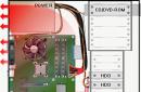
1. Unbuffered memory . Regular memory for regular desktop computers, it is also called UDIMM. A memory stick usually has 2, 4, 8 or 16 memory chips on one or both sides. For such memory, the marking usually ends with the letter U (Unbuffered) or without a letter at all, for example DDR2 PC-6400, DDR2 PC-6400U, DDR3 PC-8500U or DDR3 PC-10600. And for laptop memory, the marking ends with the letter S, apparently this is an abbreviation for SO-DIMM, for example DDR2 PC-6400S. A photo of unbuffered memory can be seen below.
2. Error Correcting Memory (ECC memory). Regular unbuffered memory with error correction. Such memory is usually installed in branded computers sold in Europe (NOT SERVERS), the advantage of this memory is its greater reliability during operation. Most memory errors can be corrected during operation, even if they appear, without losing data. Typically, each stick of such memory has 9 or 18 memory chips; one or 2 chips are added. Most regular computers (not servers) and motherboards can handle ECC memory. For such memory, the marking usually ends with the letter E (ECC), for example DDR2 PC-4200E, DDR2 PC-6400E, DDR3 PC-8500E or DDR3 PC-10600E. A photo of unbuffered ECC memory can be seen below.
The difference between memory with ECC and memory without ECC can be seen in the photo:
Although most boards sold support this memory, it is better to find out compatibility with a specific board and processor in advance before purchasing. From personal experience, 90-95% of motherboards and processors can handle ECC memory. Among those that cannot work: boards based on Intel G31, Intel G33, Intel G41, Intel G43, Intel 865PE chipsets. All motherboards and processors starting from the first generation Intel Core can all work with ECC memory and this does not depend on the motherboard. For AMD processors, in general, almost all motherboards can work with ECC memory, except for cases of individual incompatibility (this happens in the rarest cases).
3. Register memory (Registered). SERVER memory type. Usually he always released with ECC(error correction) and with a "Buffer" chip. The “buffer” chip allows you to increase the maximum number of memory sticks that can be connected to the bus without overloading it, but this is unnecessary data, we will not delve into the theory. Recently, the concepts buffered and registered are almost not distinguished. To exaggerate: register memory = buffered. This memory works ONLY on server motherboards capable of working with memory using a “buffer” chip.
Typically, register memory strips with ECC have 9, 18 or 36 memory chips and another 1, 2 or 4 “buffer” chips (they are usually in the center and differ in size from the memory chips). For such memory, the marking usually ends with the letter R (Registered), for example DDR2 PC-4200R, DDR2 PC-6400R, DDR3 PC-8500R or DDR3 PC-10600R. Also in the marking of register (server) (buffered) memory there is usually an abbreviation for the word Registered - REG. A photo of buffered (registered) memory with ECC can be seen below.
Remember! Registered memory with ECC is 100% likely NOT to work on regular motherboards. It only works on servers!
4. FB-DIMM Fully Buffered DIMM(Fully Buffered DIMM) is a computer memory standard that is used to improve the reliability, speed, and density of the memory subsystem. In traditional memory standards, data lines are connected from the memory controller directly to the data lines of each DRAM module (sometimes through buffer registers, one register chip per 1-2 memory chips). As the channel width or data transfer rate increases, the signal quality on the bus deteriorates and the bus layout becomes more complicated. This limits memory speed and density. FB-DIMM takes a different approach to solve these problems. This is a further development of the idea of registered modules - Advanced Memory Buffer buffers not only address signals, but also data, and uses a serial bus to the memory controller instead of a parallel one.
The FB-DIMM has 240 pins and is the same length as other DDR DIMMs, but differs in the shape of the tabs. Suitable for server platforms only.
FB-DIMM specifications, like other memory standards, are published by JEDEC.
Intel used FB-DIMM memory in systems with Xeon 5000 and 5100 series processors and later (2006-2008). FB-DIMM memory is supported by server chipsets 5000, 5100, 5400, 7300; only with Xeon processors based on the Core microarchitecture (socket LGA771).
In September 2006, AMD also abandoned plans to use FB-DIMM memory.
If you find it difficult to choose memory for your computer, check with the seller and tell him the motherboard model and processor model.
P.S.: Recently, another cheap and interesting type of memory has appeared - I call it “Chinese Counterfeit”. For those who haven't encountered it yet, I'll tell you. This is the kind of memory that can always be recognized by its contacts; usually they are oxidized, and even if they are cleaned, within a month or two they oxidize again, become cloudy, dirty, and the memory may malfunction or not work at all. There is not even a smell of gold on the contacts of this memory. Another difference between this memory and the original one is that it works on certain motherboards or processors, for example ONLY on AMD, or only strictly on some chipsets. Moreover, the list of these chipsets is very small. What is the secret of this “memory” is not yet clear to me, but many people buy it - after all, it is 40-50% cheaper than a similar one. And what’s most surprising is that the new “Chinese Counterfeit” usually costs less than the original used memory :) I won’t talk about the reliability and durability of the work, everything is clear here.
Registered Memory RDIMM , Sometimes buffered memory listen)) is a type of computer RAM whose modules contain a register between the memory chips and the system memory controller. The presence of registers reduces the electrical load on the controller and allows you to install more memory modules in one channel. Register memory is more expensive due to lower production volume and the presence of additional chips. Typically used in systems that require scalability and fault tolerance at the expense of low cost (for example, in servers). Although most memory modules for servers are registered and use ECC, there are also modules with ECC but without registers (UDIMM ECC), they are also in most cases functional in desktop systems. There are no register modules without ECC.The use of registers introduces additional latency when accessing memory. Each read and write is buffered in the register for one clock cycle before reaching the DRAM chip from the memory bus, so registered memory is considered one clock cycle slower than non-register memory ( UDIMM,unregistered DRAM). For SDRAM memory, this delay is significant only for the first cycle in a series of requests (burst).
Only control and address signals are buffered in register memory.
Buffered memory ( Buffered memory) is an older term for register memory.
Some newer systems use fully buffered FB-DIMM memory, which buffers not only the control lines, but also the data lines using a special AMB controller located on each memory module.
Registered memory technique can be applied to different generations of memory, for example: DDR DIMM, DDR2 DIMM, DDR3 DIMM
Write a review about the article "Register memory"
Notes
Literature
- Memory systems: cache, DRAM, disk; Section 10.3.3 Registered Memory Module (DIMM)
Links
- // ixbt
| This is a preliminary article about computer technology. You can help the project by adding to it. |
An excerpt characterizing register memory
- Fool! beast! - Pierre shouted, which rarely happened to him, cursing his coachman. - I ordered home; and hurry up, you idiot. “We still have to leave today,” Pierre said to himself.Pierre, seeing the punished Frenchman and the crowd surrounding the Execution Ground, so finally decided that he could not stay any longer in Moscow and was going to the army that day, that it seemed to him that he either told the coachman about this, or that the coachman himself should have known it .
Arriving home, Pierre gave an order to his coachman Evstafievich, who knew everything, could do everything, and was known throughout Moscow, that he was going to Mozhaisk that night to the army and that his riding horses should be sent there. All this could not be done on the same day, and therefore, according to Evstafievich, Pierre had to postpone his departure until another day in order to give time for the bases to get on the road.
On the 24th it cleared up after the bad weather, and that afternoon Pierre left Moscow. At night, after changing horses in Perkhushkovo, Pierre learned that there had been a big battle that evening. They said that here, in Perkhushkovo, the ground shook from the shots. No one could answer Pierre's questions about who won. (This was the battle of Shevardin on the 24th.) At dawn, Pierre approached Mozhaisk.
All the houses of Mozhaisk were occupied by troops, and at the inn, where Pierre was met by his master and coachman, there was no room in the upper rooms: everything was full of officers.
In Mozhaisk and beyond Mozhaisk, troops stood and marched everywhere. Cossacks, foot and horse soldiers, wagons, boxes, guns were visible from all sides. Pierre was in a hurry to move forward as quickly as possible, and the further he drove away from Moscow and the deeper he plunged into this sea of troops, the more he was overcome by anxiety and a new joyful feeling that he had not yet experienced. It was a feeling similar to the one he experienced in the Slobodsky Palace during the Tsar’s arrival - a feeling of the need to do something and sacrifice something. He now experienced a pleasant feeling of awareness that everything that constitutes people’s happiness, the comforts of life, wealth, even life itself, is nonsense, which is pleasant to discard in comparison with something... With what, Pierre could not give himself an account, and indeed she tried to understand for himself, for whom and for what he finds it especially charming to sacrifice everything. He was not interested in what he wanted to sacrifice for, but the sacrifice itself constituted a new joyful feeling for him.
There are two main types of random access memory (RAM); These are buffered memory - or register memory - and unbuffered memory. Unbuffered memory is faster, and often significantly cheaper, than buffered memory. Thus, it is a type of module that can be found in almost all home desktop and laptop computers. Buffered memory is more expensive than the unbuffered type, and it is also slower due to the way it handles storing and restoring data.
Buffered memory, however, is much more stable than unbuffered forms, which is why it is used primarily on mainframe computers and servers.
Unbuffered memory is by far the most common form of computer memory module found in everyday use. These memory modules are cheap to produce compared to buffered memory modules, partly due to their common use in home and commercial computers and also because less hardware is used. An unbuffered memory module does not have any built-in hardware to act as an instruction register between the RAM chip and the computer's memory controller. This results in faster performance, but increases the risk of critical memory loss errors that occur due to the random nature of information placement and retrieval, especially during periods of intense activity.
Most commonly referred to as registered memory is buffered memory. Unbuffered memory, oddly enough, retained its name and was not changed to unregistered memory. Buffered memory differs from the unbuffered type in that it has a hardware register that stores information in the cache during one clock cycle of the memory chip. Although this operation may result in slower memory chip runtime, it provides additional stability and reduces the risk of memory errors.
In general household use, the difference in speed between the two types of memory modules seems negligible. During periods of intense information exchange, the latency observed using the register appears. Buffered memory is commonly used in server computers and mainframe systems to provide stability and protection against corruption that can occur in unbuffered modules when they are subject to constant heavy use. Although buffered modules are more expensive and generally slower to operate, memory stability and data security more than make up for it in a production environment.